

Lateral bipolar field effect mode hybrid transistor and method for operating the same
- Summary
- Abstract
- Description
- Claims
- Application Information
AI Technical Summary
Benefits of technology
Problems solved by technology
Method used
Image

Examples
Embodiment Construction
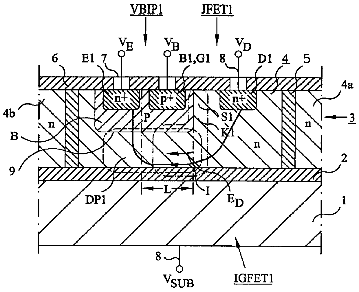
The problem of a high-voltage vertical transistor is that a relatively thick buried oxide layer is needed, about 3 .mu.m, below an active epi-layer to suppress the dependence on substrate potential. This results in problems with heat diversion from the transistor in the epi-taxial layer. A very high accuracy is further required regarding the epi-layer's thickness and resistivity, depending on the doping of the epi-layer. Further, it is hard to find manufacturers fulfilling the requirements above regarding accuracy. The present invention relates to the above problems.
A further problem is to achieve a predetermined high gain in connection with voltage durability and external control of the gain of a bipolar component.
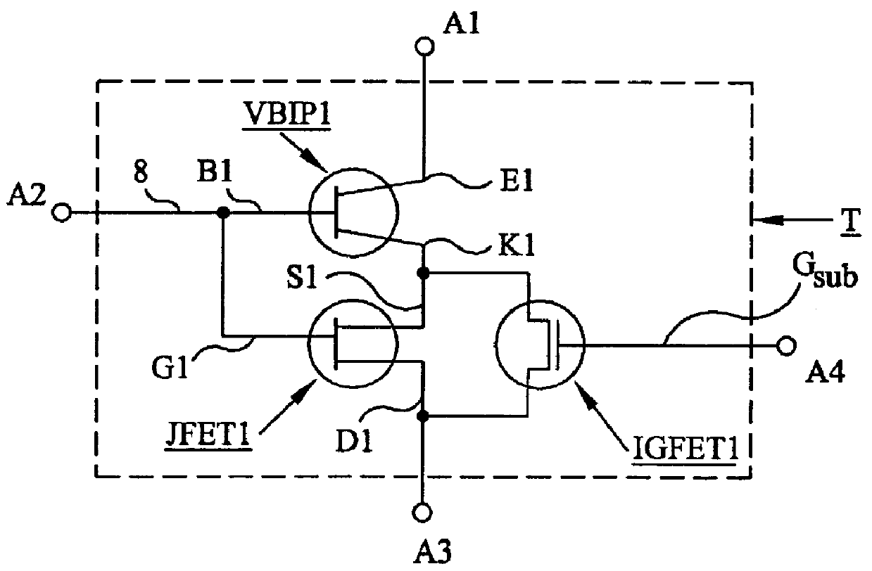
A not previously addressed new problem is how to make a semiconductor device which can be set up to work in two different modes, such as different components of conventional type, e.g. from a lateral bipolar transistor to a MOS.
The object of the present invention is to re...
PUM
 Abstract
Description
Claims
Application Information