

Semiconductor structure useful in a self-aligned contact having multiple insulation layers of non-uniform thickness
a technology of self-aligning contact and semiconductor structure, which is applied in the direction of semiconductor/solid-state device details, semiconductor devices, electrical apparatus, etc., can solve the problems of inability failure to meet the requirements of the application, and undetectable thinness in the lower corners and bottoms of tight areas
- Summary
- Abstract
- Description
- Claims
- Application Information
AI Technical Summary
Problems solved by technology
Method used
Image

Examples
Embodiment Construction
The following examples are included to demonstrate preferred embodiments of the invention. It should be appreciated by those skilled in the art that the techniques disclosed in the examples that follow represent techniques discovered by the inventor to function well in the practice of the invention, and thus can be considered to constitute preferred modes for its practice. However, those skilled in the art should, in light of the present disclosure, appreciate that many changes can be made in the specific embodiments disclosed herein and still obtain a like or similar result without departing from the spirit and scope of the invention.
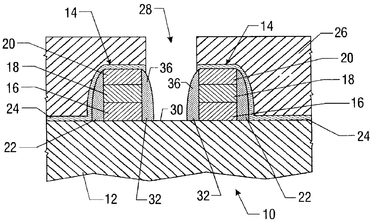
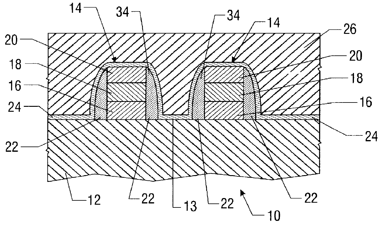
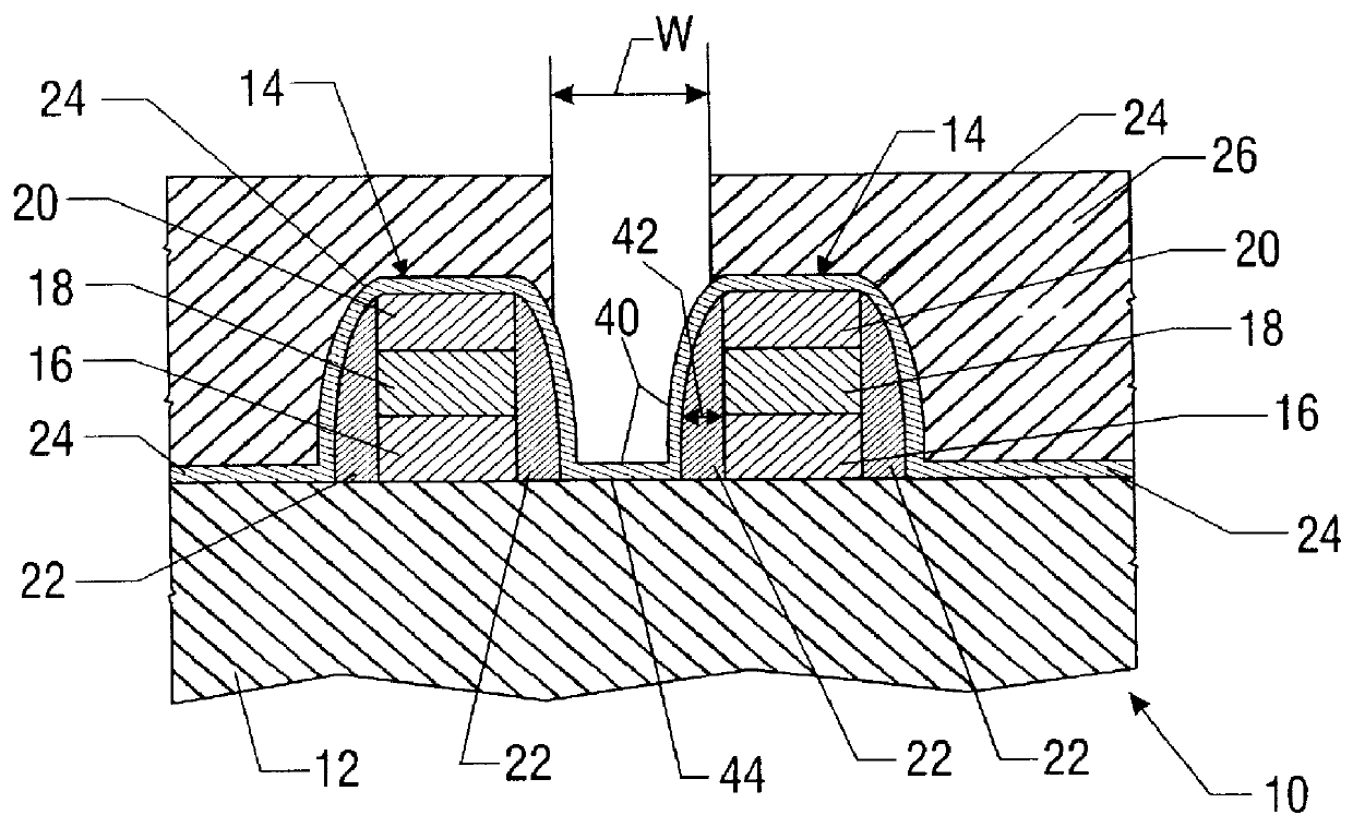
Referring to FIG. 5, a portion of a semiconductor wafer 50 is shown. The wafer 50 has a substrate 52 with a top surface 54 on which conventional patterning and etching has formed two multilayered structures 56. The substrate 50 may be any suitable material known to the art and may be a wafer or a previously deposited oxide layer. The multilayered struc...
PUM
 Abstract
Description
Claims
Application Information