Gated clock tree synthesis method for the logic design

a logic design and clock tree technology, applied in the field of gated clock tree synthesis methods, can solve the problems of inability to synthesize gated clock buffers, complex design and difficulty for designers, and the transmission of clock signals from one point to another can suffer from distortion

Inactive Publication Date: 2000-02-01
VIA TECH INC
View PDF3 Cites 54 Cited by
  • Summary
  • Abstract
  • Description
  • Claims
  • Application Information

AI Technical Summary

Problems solved by technology

One drawback of the conventional CTS methods, however, is that they can be used only to synthesize on gated buffer, and is unable to synthesize gated clock buffer.
Due to this drawback, the required logic gates in a buffer need to be additionally provided by the designer, which makes the design very complex and difficult for the designer.
Besides, the transmission of the clock signals from one point to another can suffer from distortions due to lengthy transmission paths in cases where a gated clock signal is used to drive latches or registers, since a single buffer can be used for the transfer of various gated clock signals or non-gated clock signals.
One drawback to the foregoing logic circuits, however, is that they may fail to provide optimal localization of the logic elements in the gate array such that the signal transmission can suffer from an increased time delay that degrades the performance of the circuit.
The time delay in the control signal transferred over the lengthy line can thus be large, which degrades the performance of the logic circuit.

Method used


Image

  • Gated clock tree synthesis method for the logic design
  • Gated clock tree synthesis method for the logic design
  • Gated clock tree synthesis method for the logic design

Examples


Embodiment Construction

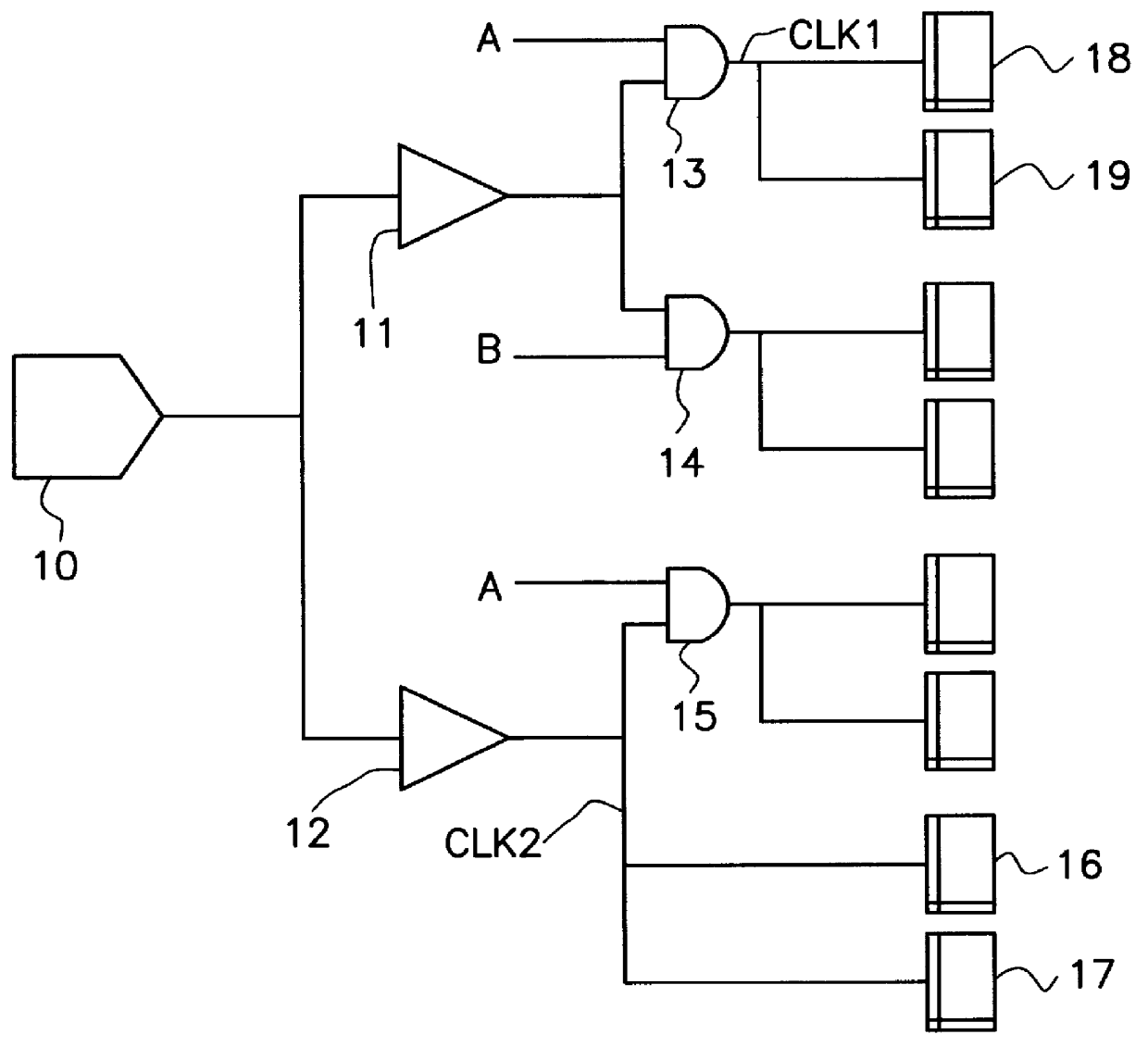
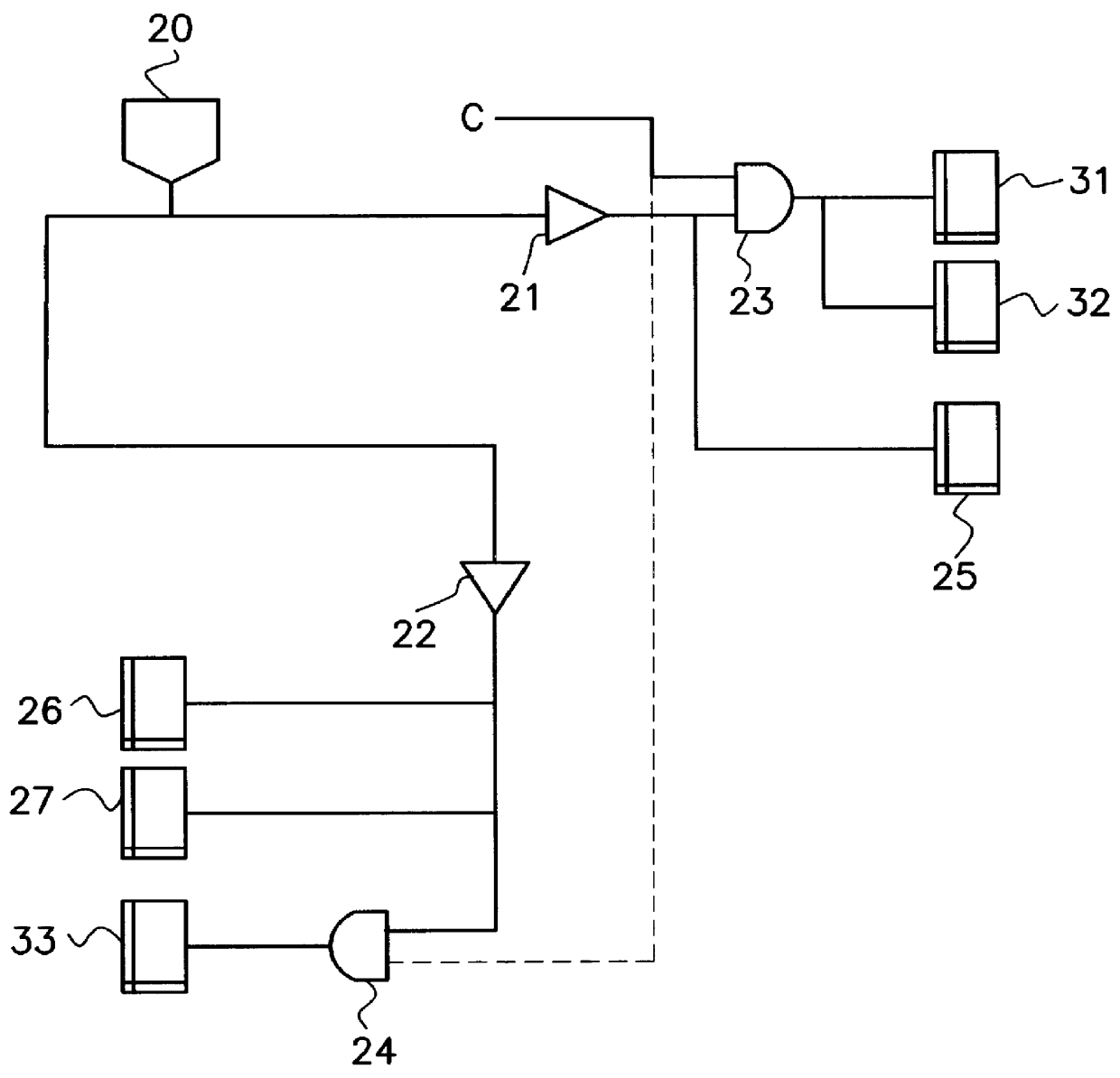
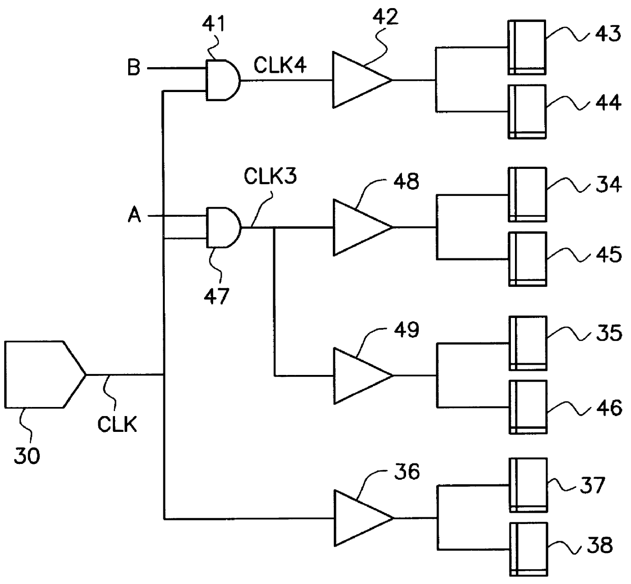
In the design of a logic circuit in accordance with the method of the invention, those logic elements in the logic circuit that are to be driven by the same gated clock signal are grouped into the same group and then arranged together as a collective unit in the same circuit layout area. For example, those logic elements that are to be driven by a first gated clock signal enabled by a first control signal are grouped into a first group. Those logic elements driven by a second gated clock signal enabled by a second control signal are grouped into a second group, and so forth. Further, those logic elements that are driven continuously without interruption by the system clock signal are grouped into another group. Each group of logic elements are arranged together as a collective unit in the same circuit layout area without being intermixedly arranged with those logic elements in other groups. This design scheme allows the gates to be arranged in an orderly fashion, making the design l...


PUM


Abstract

A gated clock tree synthesis (CTS) method is provided for the purpose of synthesizing a gate array logic circuit to allow optimal topological arrangement of the gate array on the logic circuit. This in turn allows the logic circuit to operate more efficiently. The logic circuit includes at least one clock generator, a plurality of control gates each having one input end connected to a control signal and the other input end connected to receive the output clock signal from the clock generator, a plurality of first logic elements that are directly driven by the output clock signal from the clock generator, and a plurality of second logic elements that are driven by the gated clock signal outputted from each of the control gates under control by the control signal. The gated CTS method comprises the steps of grouping the first logic elements into a plurality of groups, connecting each group of the first logic elements via a first buffer to one of the control gates, connecting each of the second logic elements via a second buffer to the clock generator, and connecting one input end of each of the control gates to the clock generator.

Description

This application claims the priority benefit of Taiwan application serial no. 87102972, filed Mar. 2, 1998, the full disclosure of which is incorporated herein by reference.1. Field of the InventionThis invention relates to clock tree synthesis (CTS) methods, and more particularly, to a gated CTS method which can help make the design of a gate array logic circuit less complex and less difficult for the designer, and which can make the resultant logic circuit more efficient in clocking performance.2. Description of Related ArtIn the manufacture of logic circuits, a common practice is the utilization of the so-called ASIC (application-specific integrated circuit) technology. ASIC technology involves fabrication of a special type of chip as a nonspecific collection of logic gates, and later in the manufacturing process, addition of a layer connecting the gates so as to provide the specified logic function. Where efficient power management is desired, the conventional gated CTS methods ...

Claims


Application Information

Patent Timeline
Patent Type & Authority Patents(United States)
IPC IPC(8): G06F1/10G06F17/50
CPCG06F1/10G06F17/505G06F2217/62G06F30/327G06F30/396G06F2117/04
Inventor CHIU, YOU-MINGLAI, JIIN
Owner VIA TECH INC
Why Eureka
Try Eureka