
Method of forming mask ROM

a mask rom and mask technology, applied in the field of mask roms, can solve the problem that the data stored in the mask rom cannot be changed, and achieve the effect of improving the quality of mask roms and reducing the size of mask roms

Inactive Publication Date: 2000-02-08
LG SEMICON CO LTD
View PDF12 Cites 14 Cited by
  • Summary
  • Abstract
  • Description
  • Claims
  • Application Information

AI Technical Summary

Problems solved by technology

Data stored in a mask ROM is not able to be changed, rather it is only possible to read the data.

Method used


Image

  • Method of forming mask ROM
  • Method of forming mask ROM
  • Method of forming mask ROM

Examples


Embodiment Construction

Reference will now be made in detail to the preferred embodiments of the present invention, examples of which are illustrated in the accompanying drawings.

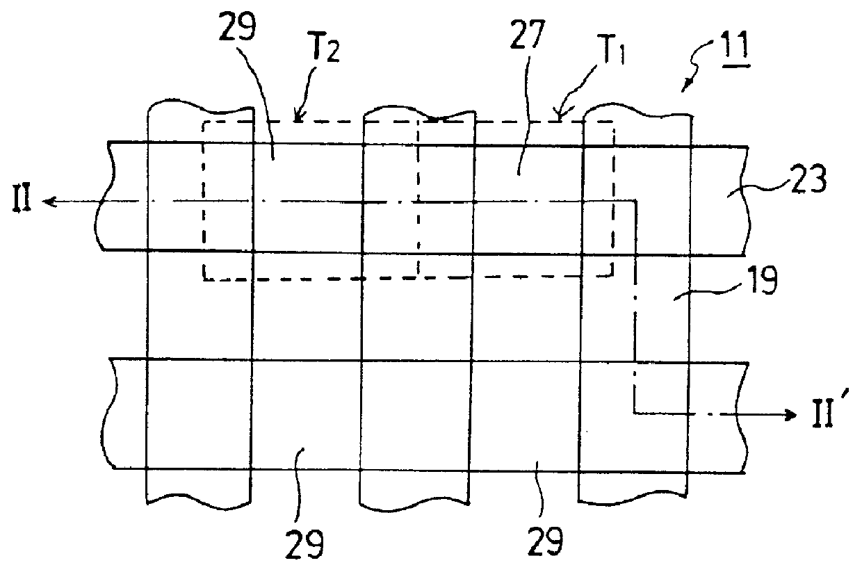
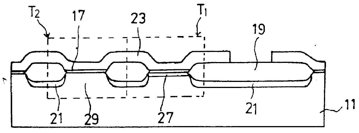
As illustrated in FIG. 4, in a mask ROM of the invention, there is a semiconductor substrate 31 on which a trench 35 is formed. A buried oxide layer 41 is formed on the part where the trench 35 is not formed, and under the bottom surface of the trench 35. A high concentration impurity region (see reference numeral 43 in FIG. 5) made of a common source and drain region and used for a bit line, is formed under the buried oxide layer 41. A word line, functioning as a gate 45, is formed perpendicular to the buried oxide layer 41. In forming the transistors by intersecting the word line 45 with the bit line 43 shown in FIG. 5 below layer 41, one side of the trench 35 overlapping with the gate 45 becomes the first and second channels 51 and 53 of the first and second transistors T11 and T12. The first channel 51 is coded by doping with ...


PUM


Abstract

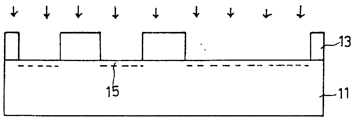
A method of fabricating a mask ROM includes forming a trench on a first conductivity type semiconductor substrate, implanting a second conductivity type impurity ion in at least a surface portion of the semiconductor substrate where the trench is formed, forming an insulating oxide layer on a surface of the semiconductor substrate, including a surface of the trench, forming gate oxide layers of both sides of the trench, forming first and second gates on the gate oxide layers and forming a first conductivity type channel by implanting a first conductivity type impurity ion in one side of the trench. As such, the resulting mask ROM includes two transistors on either side of a trench having channels along the side walls of the trench. The resulting mask ROM has a reduced surface width, enhancing integration.

Description

1. Field of the InventionThe present invention relates to a mask ROM and its fabrication method and, more particularly, to a mask ROM capable of continuously coding data by implanting ions, using a mask of a user during the fabricating process.2. Discussion of Related ArtA ROM is a nonvolatile memory device in which stored data are not changed in a normal operation state. A ROM is classified according to the methods for storing data into the ROM. There are a mask read only memory (ROM), a programmable ROM (PROM), an electrically programmable ROM (EPROM) and an erasable and electrically programmable ROM (EEPROM).The mask ROM is coded with its data, i.e., has its data stored in it, by using a specialized mask (representing particular required for a user) during the fabrication process. Data stored in a mask ROM is not able to be changed, rather it is only possible to read the data. A type of mask ROM causes a predetermined transistor have a status that differs from other transistors b...

Claims


Application Information

Patent Timeline
IPC IPC(8): H01L21/70H01L21/8246H01L27/112G11C17/08
CPCH01L27/11273H10B20/40H01L21/823487
Inventor SHIN, BONG-JOLEE, KI-JIK
Owner LG SEMICON CO LTD
Learn More