Salicide formation process

a technology of sulfuric acid and formation process, which is applied in the direction of semiconductor devices, electrical equipment, basic electric elements, etc., can solve the problems of reducing the performance of mos and other types of integrated circuits, undetectable polysilicon electrodes that form the gates of mos devices and wiring lines within semiconductor devices, and prolonging the rc time constan

Inactive Publication Date: 2000-02-08
UNITED MICROELECTRONICS CORP
View PDF5 Cites 23 Cited by
  • Summary
  • Abstract
  • Description
  • Claims
  • Application Information

AI Technical Summary

Problems solved by technology

As line widths and geometries for semiconductor devices are made smaller, the polysilicon electrodes that form the gates of MOS devices and wiring lines within semiconductor devices become undesirably resistive.
For smaller line widths, even highly doped polysilicon is sufficiently resistive to diminish the performance of MOS and other types of integrated circuits which include polysilicon electrodes or which otherwise incorporate polysilicon electrodes because the resistivity of the polysilicon reduces signal levels and produces longer RC time constants in the associated circuits.
The formation of stringers 32 is obviously undesirable in that the stringers short the gate to the source/drain regions and render the trans...

Method used


Image

  • Salicide formation process
  • Salicide formation process
  • Salicide formation process

Examples


Embodiment Construction

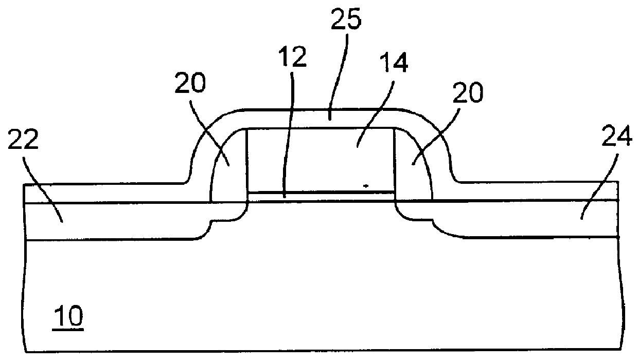
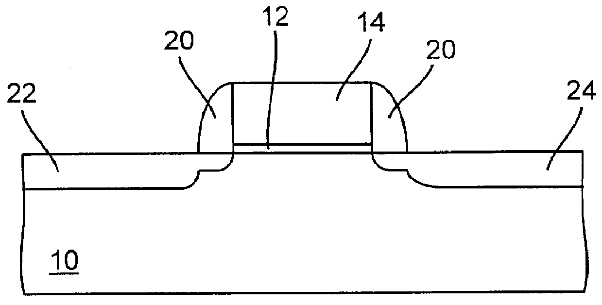
One embodiment of the present invention relates to a method of forming a self-aligned silicide structure including forming a structure including a layer of titanium over a gate electrode and over source / drain regions in a substrate. Direct sputtering is used to deposit a layer of titanium nitride over the layer of titanium using a titanium nitride target material. The structure is annealed at a first temperature to form titanium silicide on the polysilicon gate electrode and titanium silicide on the source / drain regions, and the titanium nitride is removed from the structure.

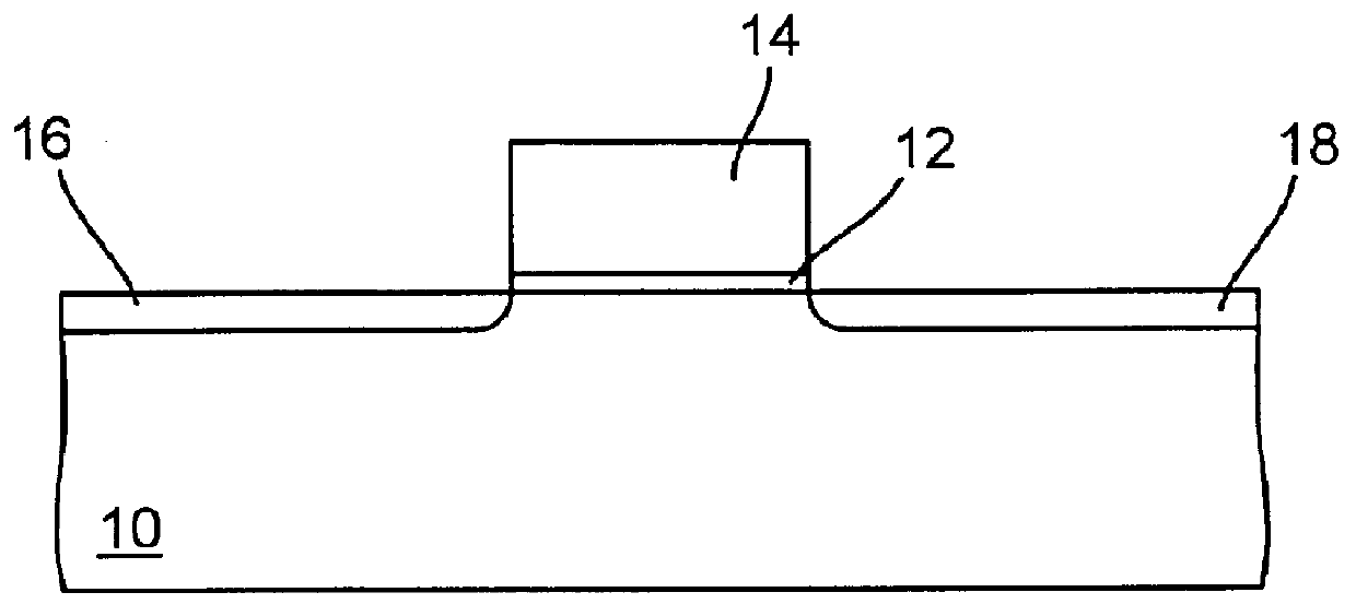
Other embodiments relate to a method of making a semiconductor device including a MOS transistor. An insulator is formed on a semiconductor substrate and a gate electrode formed on the insulator. Source / drain regions are formed within the substrate on either side of the gate electrode. A layer of titanium is direct sputtered the semiconductor device, and a layer of nitride is direct sputtered over the titanium l...


PUM


Abstract

A method of making a semiconductor device including a MOS transistor provides an insulator formed on a semiconductor substrate and a gate electrode formed on the insulator. Source/drain regions are formed within the substrate on either side of the gate electrode. A layer of titanium is sputtered onto the semiconductor device, and a layer of titanium nitride is direct sputtered over the titanium layer using a titanium nitride target. The device is annealed at a first temperature to form a structure including titanium silicide on the polysilicon electrode, titanium silicide on the surface of the source/drain regions, unreacted titanium over the silicide regions, and titanium nitride over the unreacted metal. The unreacted titanium and titanium nitride are removed from the structure, and the structure is annealed at a higher temperature than the first temperature to form a lower resistivity titanium silicide.

Description

1. Field of the InventionThe present invention relates to the fabrication of semiconductor devices incorporating structures including of a layer of polysilicon covered by a self-aligned layer of metal silicide.2. Description of the Related ArtAs line widths and geometries for semiconductor devices are made smaller, the polysilicon electrodes that form the gates of MOS devices and wiring lines within semiconductor devices become undesirably resistive. Multilayer electrodes in which a layer of polysilicon is covered by one or more layers of metals or metal silicides are used to provide electrodes having a lower resistance than electrodes consisting solely of polysilicon. Silicide electrodes may consist, for example, of a layer of polysilicon having a thickness of approximately 1000 .ANG. to 3000 .ANG. covered by titanium silicide or another metal silicide having a thickness of greater than 100 .ANG.. The silicide layer provided on the polysilicon layer acts as a lower resistance condu...

Claims


Application Information

Patent Timeline
IPC IPC(8): H01L21/285H01L21/336H01L21/02H01L21/28
CPCH01L21/28052H01L21/28518H01L29/665
Inventor CHEN, TUNG-POPAN, HONG-TSZHSIEH, WEN-YI
Owner UNITED MICROELECTRONICS CORP
Why Eureka
Try Eureka