Ring oscillators having inverting and delay elements

a delay element and oscillator technology, applied in the field of oscillator circuits, can solve the problems of poor control property and inability to increase the frequency range of the oscillator

Inactive Publication Date: 2000-02-22
SONY CORP
View PDF1 Cites 50 Cited by
  • Summary
  • Abstract
  • Description
  • Claims
  • Application Information

AI Technical Summary

Problems solved by technology

As a result, in the oscillator circuit of the related art, there were the disadvantages that the control property was poor and the range of variation of the frequency could not be increased.

Method used


Image

  • Ring oscillators having inverting and delay elements
  • Ring oscillators having inverting and delay elements
  • Ring oscillators having inverting and delay elements

Examples


first embodiment

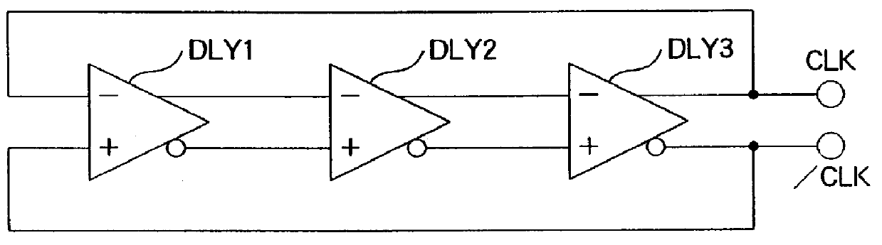
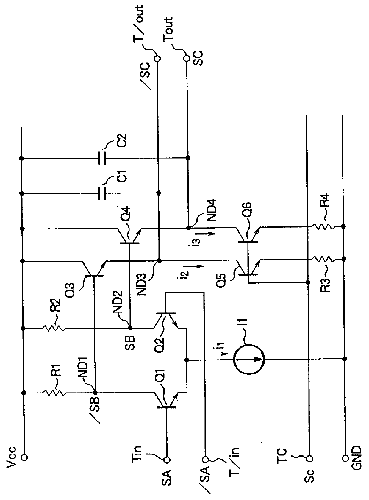
FIG. 4 is a circuit diagram of the configuration of an inverting delay circuit DLY1 of a constituent element of the oscillator circuit according to the present invention.

As illustrated, the inverting delay circuit DLY1 is constituted by inverting elements comprising differential amplifier circuits and delay elements comprising emitter followers and capacitors.

The differential amplifier circuit is constituted by the transistors Q1 and Q2, the resistance element R1, and the current source I1. Bases of the transistors Q1 and Q2 are respectively connected to the input terminals Tin and T / in, the collector of the transistor Q1 is connected to the supply line of the power supply voltage V.sub.CC via the resistance element R1, and the collector of the transistor Q2 is connected to the supply line of the power supply voltage V.sub.CC. The emitters of the transistors Q1 and Q2 are commonly connected to the current source I1. The connection node ND1 of the collector of the transistor Q1 and t...

second embodiment

FIG. 6 is a circuit diagram of the configuration of the non-inverting delay circuit DLY2 of another constituent element of the oscillator circuit according to the present invention.

As illustrated, the non-inverting delay circuit DLY2 is constituted by a non-inverting element (hereinafter referred to as a "buffer") comprising a differential amplifier circuit and a delay element comprising an emitter follower and a capacitor.

The differential amplifier circuit is constituted by the transistors Q1 and Q2, the resistance element R1, and the current source I1. Bases of the transistors Q1 and Q2 are respectively connected to the input terminals Tin and T / in, the collector of the transistor Q2 is connected to the supply line of the power supply voltage V.sub.CC via the resistance element R2, and the collector of the transistor Q1 is connected to the supply line of the power supply voltage V.sub.CC. The emitters of the transistors Q1 and Q2 are commonly connected to the current source I1. Th...

third embodiment

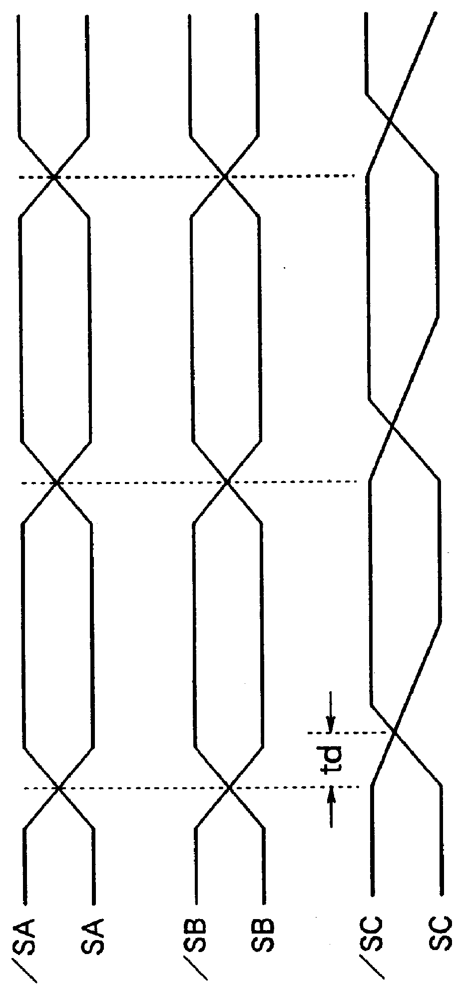
Below, an explanation will be made of a ring oscillator circuit constituted by using the inverting and non-inverting delay circuits of the basic circuits of the present invention mentioned above.

First, the equivalent circuit of the inverting delay circuit and the non-inverting delay circuit of the constituent elements of the present invention is as shown in FIGS. 8A and 8B.

The equivalent circuit of the inverting delay circuit is shown in FIG. 8A, and the equivalent circuit of the non-inverting delay circuit is shown in FIG. 8B. As illustrated, the inverting delay circuit is equivalently constituted by an inverter INV0 and a delay element D0. The inverter INV0 is constituted by for example a differential amplifier circuit as shown in FIG. 4, and the delay element D0 is constituted by for example an emitter follower and a capacitor and, further, the comparison circuit. The non-inverting delay circuit is equivalently constituted by a buffer BUF0 and the delay element D0. The buffer BUF...


PUM


Abstract

An oscillator circuit constituted by connecting in a ring an odd number of stages of inverting delay circuits comprising inverting elements, for example, inverters INV1, INV2, and INV3, and delay elements D1, D2, and D3 connected to the output terminals of the inverting elements. In each delay element, the capacitor is charged and discharged in accordance with the output signal level from the inverter, the voltage of the capacitor and the reference voltage are compared by a comparison circuit, and a signal in accordance with the result of comparison is input to the inverting delay circuit of the next stage, therefore the delay time can be controlled by controlling the charging current of the delay element and the oscillation frequency can be controlled in accordance with this. Accordingly, the control property thereof is good, the range of variation can be broadened, and a reduction of jitter can be realized.

Description

1. Field of the InventionThe present invention relates to an oscillator circuit constituted of a plurality of inverting and non-inverting delay circuits connected in the form of a ring.2. Description of the Related ArtAn oscillator circuit may be configured by connecting an odd number of inverting delay circuits, for example, the three inverting delay circuits DLY1, DLY2, and DLY3, in the form of the ring. FIG. 1 is a circuit diagram of a ring oscillator circuit constituted in this way, while FIG. 2 shows the configuration of an inverting delay circuit comprising inverting elements and delay elements connected to the output side of the inverting elements.As shown in FIG. 2, an inverting element is constituted by a differential amplifier circuit. The delay element connected to the output side thereof is constituted by a transistor and capacitor forming an emitter follower. The differential amplifier circuit is constituted by transistors Q1 and Q2, resistance elements R1 and R2, and a...

Claims


Application Information

Patent Timeline
Patent Type & Authority Patents(United States)
IPC IPC(8): H03K3/0231H03K3/00H03K3/282H03K3/03
CPCH03K3/0231H03K5/133
Inventor KOMATSU, YOSHIHIRO
Owner SONY CORP
Why Eureka
Try Eureka