Output buffer for a mixed voltage environment
a mixed voltage environment and output buffer technology, applied in the field of output buffers for mixed voltage environments, can solve problems such as failure to operate properly or damage to the transistor
- Summary
- Abstract
- Description
- Claims
- Application Information
AI Technical Summary
Problems solved by technology
Method used
Image
Examples
specific embodiments
FIG. 7 is a circuit diagram for one embodiment of a driver circuit 220 that may be used in the output buffer 200 according to the present invention. Transistors 605, 610, which are driven by the voltage V.sub.refL and the voltage V.sub.refH, respectively, are used to limit the voltage and protect these transistors from gate stress. A transistor 600 has a gate terminal coupled to the line 231. One skilled in the art will appreciate that when at least one of the transistors 600, 615 are enabled, a signal may be applied to the line 210 and sent to the peripheral device 206. Additionally, other types of driver circuits may be used without departing from the inventive concepts previously described.
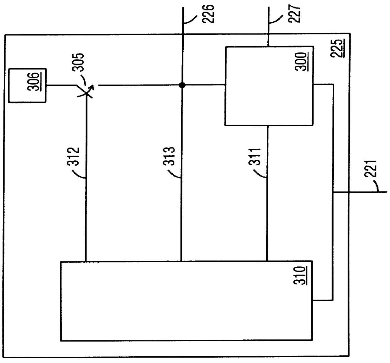
FIG. 3 is a block diagram for the level shifting circuit 225. When a signal is applied to the line 221 by the core circuit 202, it may be sent to a pull-down network 300, which may be used to apply a logically low signal to the line 226 when enabled. A switch 305 is connected to a voltage suppl...
PUM
 Abstract
Description
Claims
Application Information


