Apparatus and method for testing high speed components using low speed test apparatus

a technology of low-speed test apparatus and high-speed components, which is applied in the direction of electronic circuit testing, measurement devices, instruments, etc., can solve the problems of patents that do not teach nor disclose the internal logic testing of devices under speed test, patents that do not teach nor disclose the clock generation of test apparatuses, and patents that do not teach nor disclose the clock generation

Inactive Publication Date: 2000-04-25
IBM CORP
View PDF13 Cites 65 Cited by
  • Summary
  • Abstract
  • Description
  • Claims
  • Application Information

AI Technical Summary

Problems solved by technology

The patent does not teach nor disclose testing the internal logic of a device under test at speed.
Further, the patent does not teach nor suggest how the test apparatus clock is used to perform "at speed" tests.
However, the patent does not teach nor suggest the invention as claimed here

Method used


Image

  • Apparatus and method for testing high speed components using low speed test apparatus
  • Apparatus and method for testing high speed components using low speed test apparatus
  • Apparatus and method for testing high speed components using low speed test apparatus

Examples


Embodiment Construction

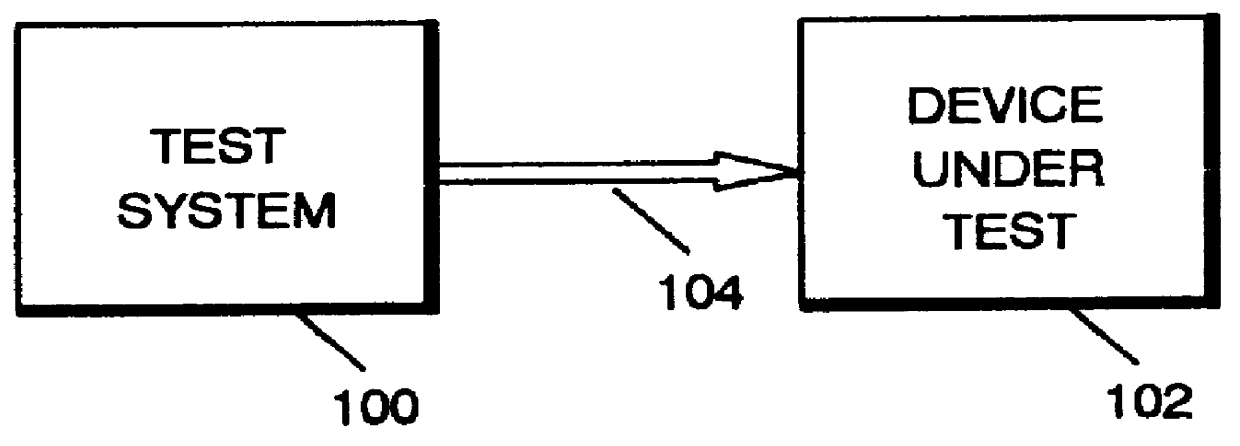
Referring now to FIG. 1, a test environment in which the present invention may be employed will be described.

A test system 100 performs tests on device under test (DUT) 102 by sending test signals to DUT 102 over lines 104.

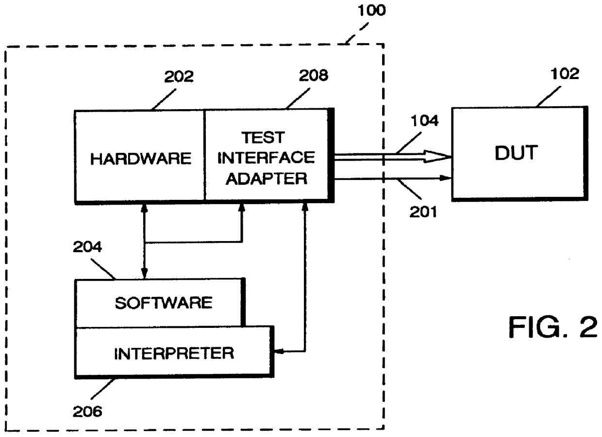
Referring now to FIG. 2, aspects of level sensitive scan design (LSSD) testing will be described as it applies to the present invention. It should be noted that LSSD testing, although employed with the present invention, is ancillary to the present invention in that the present invention is directed primarily to solving the problem of testing a high speed device with a test system which has a lower speed clocking capability.

Test system 100 may be controlled by a personal computer which includes hardware 202, software 204, an interpreter 206, and a test interface adapter 208 which communicates directly over lines 104 with device under test 102. A primary input clock CLK-PI running at the test system speed, for example, 40 Mhz, is transmitted from test system 100 to...


PUM


Abstract

A system for testing a high speed integrated circuit includes a test device having a test clock with a first maximum frequency for performing level sensitive scan design (LSSD) testing of the integrated circuit device under test, a frequency multiplier circuit for multiplying the test clock signal to a higher second frequency capable of operating the device under test, and a finite state machine for generating a first internal clock for testing the device under test. In a practical embodiment, the internal clock speed may be running at a frequency many multiples of the test clock. Alternatively, a method of testing a device under test (DUT) at design speed includes running a predetermined group of tests with a test device operating at a lower speed than the design speed; incorporating LSSD or boundary scan test techniques in the device under test, together with a frequency multiplying device; generating a global clock for the device under test from the frequency multiplying circuit and using a finite state machine as a synchronizer and pulse generator to control a capture clock with respect to the global clock.

Description

1. Field of the InventionThe present invention relates to apparatus and method for testing electronic components, and more particularly to apparatus and method for testing high speed components by test apparatus having lower speed clock capability than the high speed component being tested.2. Prior ArtIn the prior art there are many techniques for testing high speed electronic components. The following are examples of such prior art techniques.U.S. Pat. No. 5,396,170 shows an integrated test architecture which can be used in conformity with the IEEE 1149.1 test standard (JTAG) and configured on a single chip. The architecture of the patent uses the JTAG standard with additional logic on the single chip which permits "at speed" functional test of integrated circuits.Although the patent discusses tester architecture for testing an integrated circuit "at speed," the patent only shows at speed testing for boundary scan and input / output circuit testing. The patent does not teach nor disc...

Claims


Application Information

Patent Timeline
IPC IPC(8): G01R31/28G01R31/319
CPCG01R31/31903
Inventor JABER, TALAL KAMELLEBLANC, JOHNNY JAMESWALTHER, RONALD GENE
Owner IBM CORP
Why Eureka
Try Eureka