Plasma treatment method and system

a treatment method and technology of plasma, applied in the direction of electrical equipment, basic electric elements, electric discharge tubes, etc., can solve the problems of long operation time and much labor, difficult to design the system and set the process conditions, and difficult for even an expert to carry out the operation. , to achieve the effect of high inplane uniformity

Inactive Publication Date: 2000-05-23
TOKYO ELECTRON LTD
View PDF9 Cites 18 Cited by
  • Summary
  • Abstract
  • Description
  • Claims
  • Application Information

AI Technical Summary

Benefits of technology

It is therefore an object of the present invention to eliminate the aforementioned problems and to provide a method and sys

Problems solved by technology

However, since the behavior of the process has many unclear points, particularly since the history of the wafer treatment using the ECR is short, it is very difficult to design the system and to set the process conditions.
This operation needs a long time and mu

Method used


Image

  • Plasma treatment method and system
  • Plasma treatment method and system
  • Plasma treatment method and system

Examples


Embodiment Construction

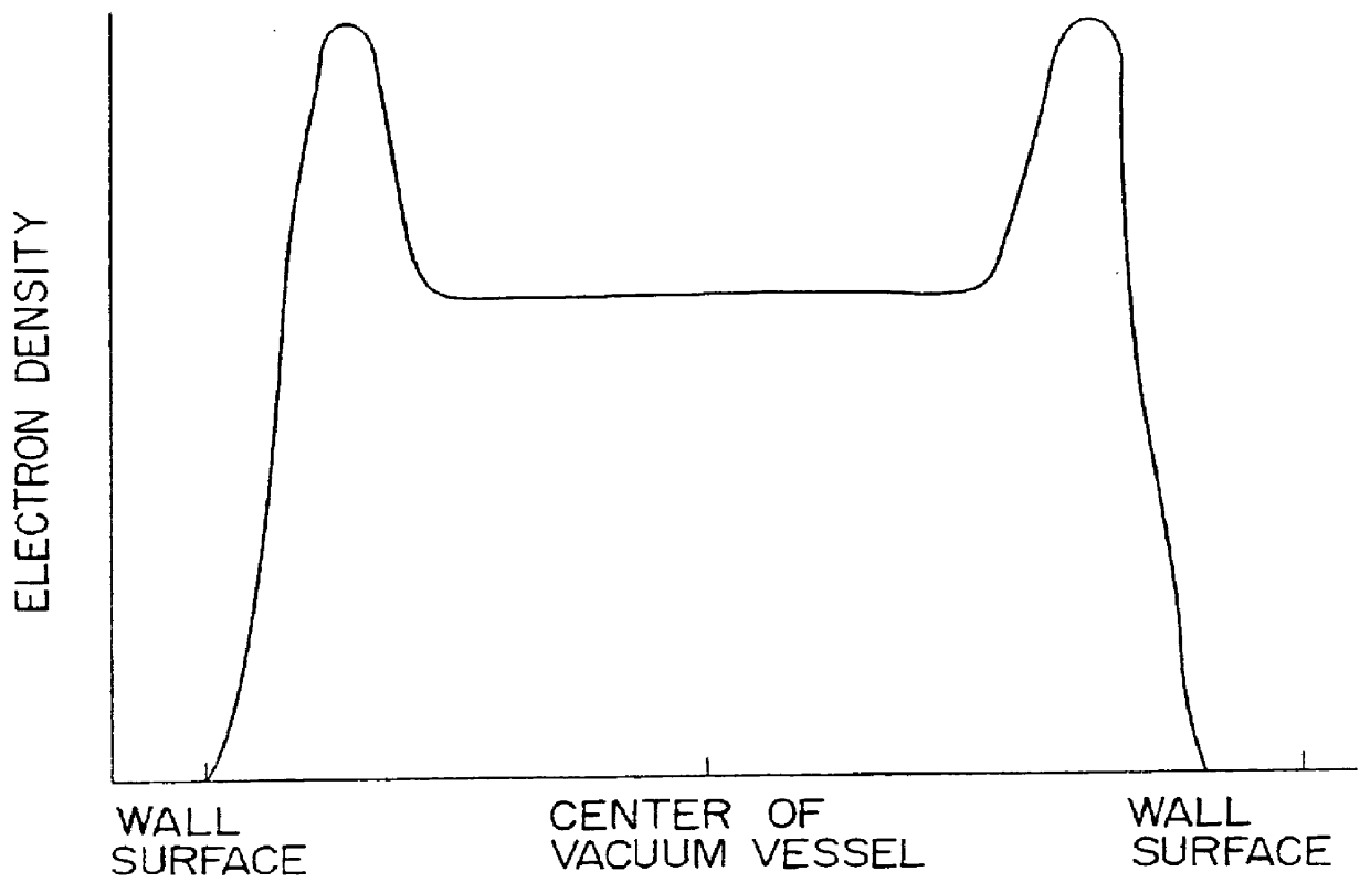
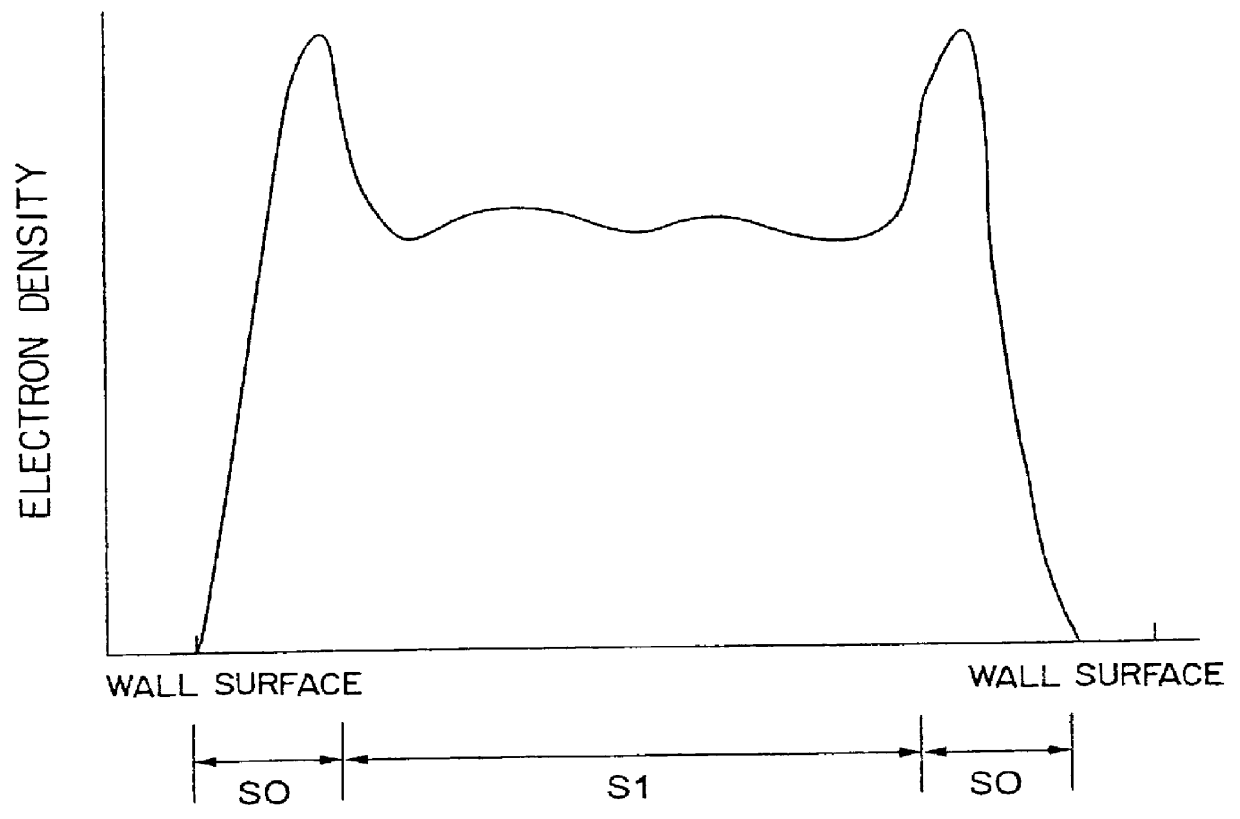
Before describing the preferred embodiments of the present invention, the fact and knowledge, on the basis of which a method according to the present invention has been made, will be described. The inventor has recognized that when the plasma treatment of a wafer is carried out by the ECR, the uniformity of a plasma treatment in the plane of a wafer, e.g., the uniformity of the thickness of a thin film in a thin film deposition process, is good if a distribution pattern of electron density, which is flat at the central portion and higher at both end portions than that at the central portion, is formed, as shown in FIG. 1, in a region, which is spaced from the wafer and which faces the wafer.

After examining what conditions and mechanisms form plasmas having such a distribution of electron density, it was found that an X wave related to the formation of such plasmas. The X wave is an elliptically polarized light wave (an electromagnetic wave) propagated across the lines of magnetic fo...


PUM


Abstract

An electron density at an ECR point, which is spaced from a substrate to be treated and which faces the substrate, is set to be higher than or equal to 0.46 nc (nc: an upper limit side cut-off density of an X wave) and lower than nc. Thus, a high chevron distribution of electron density is formed in end portions of a magnetic field forming region, and a distribution of electron density having a lower peak value than those in the end portions is formed in a central portion of the magnetic field forming region. In this case, the periphery of a magnetic field crosses the inner wall of a vacuum chamber once between the ECR point and the substrate, and a space of one fourth or more of the wavelength of the X wave is formed between the periphery of the magnetic field and the inner wall of the vacuum chamber as the magnetic field runs downstream. Thus, it is possible to achieve an inplane uniform treatment when carrying out a treatment, such as a thin film deposition or etching, with ECR plasmas for a wafer.

Description

BACKGROUND OF THE INVENTION1. Field of the InventionThe present invention relates generally to a plasma treatment method using electron cyclotron resonance, and a system using the same.2. Related Background ArtRecently, as a technique for carrying out a thin film deposition or etching with plasmas, the electron cyclotron resonance (ECR) plasma treatment method for causing a microwave discharge using a resonance phenomenon between the cyclotron motion of electrons and microwaves in a magnetic field has been widely noticed. According to this method, since high vacuum and high density plasmas can be produced by the electrodeless discharge, there are advantages in that it is possible to carry out a high-speed surface treatment and it is not likely that wafers will be contaminated.Referring to FIG. 16, an example of a conventional plasma treatment system for carrying out the ECR plasma treatment will be described by an example of a thin film deposition treatment. A microwave of, e.g., 2....

Claims


Application Information

Patent Timeline
IPC IPC(8): H01L21/02H01L21/3065
CPCH01L21/3065H01J37/32192H01J37/32678H01J37/32623H01J37/3266H01J37/321
Inventor KAWAI, YOSHINOBUUEDA, YOKOISHII, NOBUOKAWAKAMI, SATORUAMANO, HIDEAKI
Owner TOKYO ELECTRON LTD
Why Eureka
Try Eureka