High performance/high density BICMOS process

a bicmos, high-density technology, applied in the direction of semiconductor devices, basic electric elements, electrical equipment, etc., can solve the problems of not economically unfavorable such integrated circuits, the known techniques for forming integrated circuits have not utilized processing steps common to both technologies, and the known techniques for forming integrated circuits have not greatly utilized the processing steps of plural technologies. achieve the effect of high manufacturing yield and reliable operation

Inactive Publication Date: 2000-06-06
IBM CORP
View PDF26 Cites 22 Cited by
  • Summary
  • Abstract
  • Description
  • Claims
  • Application Information

AI Technical Summary

Benefits of technology

It is therefore an object of the present invention to provide a manufacturing process which can be reliably carried out at high manufacturing yields which will preserve the performance of particular circuit element (e.g. transistor) designs.
It is another object of the invention to provide a manufacturing process which can provide high integration density of circuit elements according to different technologies.
It is a further object of the invention to provide a manufacturing process of minimized complexity and number of steps by which circuit elements according to different technologies can be integrated on the same chip.
It is a yet further object of the invention to provide a manufacturing process and an integrated circuit structure, produced thereby, in which circuit elements are produced at similar levels within and above the substrate to avoid complexity of wiring formation between devices on the chip.

Problems solved by technology

At the same time, it is important that the process by which such high density integration of these devices is achieved not render such integrated circuits economically unfeasible due to the complexity of the process and reduced manufacturing yields corresponding to such complexity.
Accordingly, while so-called self-aligned and self-masking techniques are known, for the purpose of reducing the number of necessary masks and processing steps and increasing manufacturing yields, such techniques have not been greatly utilized in forming integrated circuits comprising plural technologies.
Further, known techniques for forming integrated circuits have not utilized processing steps common to both technologies for simultaneously forming portions of transistors and other elements in the different technologies.
Similarly, prior integrated circuits utilizing plural technologies often form the devices of each technology at different levels within or above the substrate, complicating wiring and manufacturing processes necessary to complete such wiring.

Method used


Image

  • High performance/high density BICMOS process
  • High performance/high density BICMOS process
  • High performance/high density BICMOS process

Examples


Embodiment Construction

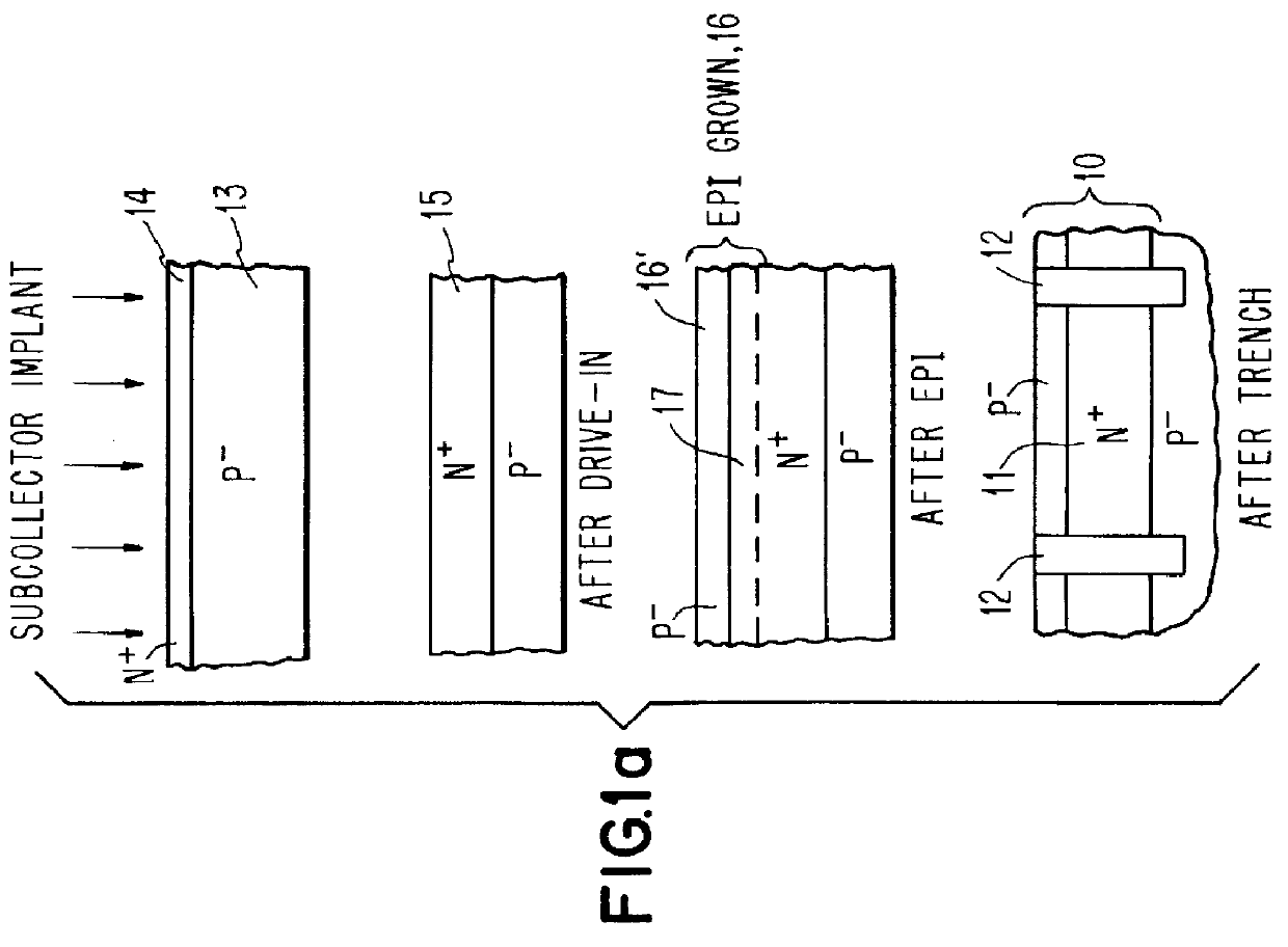
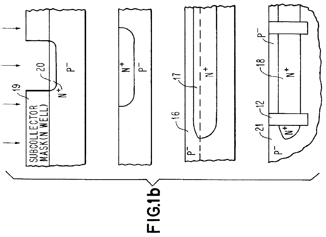
Referring now to the drawings, and more particularly to FIGS. 1a and 1b, there are shown two types of buried sub-collector structure useful with the invention and typical methods of formation of such structures. FIG. 1a particularly shows a blanket sub-collector which would typically be formed over the entirety of the chip. Trench structures 12, which are, per se, well-known for isolation of individual devices are also shown. If used only for isolation, these trench structures will be lined with an oxide and have a P+ isolation region at the bottom and a cap oxide at the top of each trench, although many different trench structures may be employed. In the preferred embodiment of the invention, at least some of the trench structures are used to make connections to the substrate of the integrated circuit although this could be done in other ways. Such a blanket sub-collector is typically formed in a P- substrate 13 by implanting an N+ impurity by any known implantation technique to fo...


PUM


Abstract

An integrated circuit using high-performance bipolar and CMOS transistor elements on a single chip is fabricated by a simplified process requiring minimal, if any, changes in the process used for forming either type of device in accordance with a variety of possible device designs. The method according to the invention makes maximal use of self-aligned and self-masking processes to reduce the number of processing steps. The number of processing steps is further reduced by performing some steps concurrently on different device types. Further, the masking steps which are employed are reasonably misregistration tolerant, resulting in high manufacturing yield for the process. Consequently, the process according to the invention substantially eliminates the existence of trade-offs between element performance, integration density and process complexity and cost when plural technologies are integrated on the same chip.

Description

BACKGROUND OF THE INVENTION1. Field of the InventionThe present invention generally relates to the manufacture of semiconductor devices and, more particularly, to the manufacture of semiconductor devices having both high-performance CMOS devices and high-performance bipolar devices integrated on a single chip at high density.2. Description of the Prior ArtHigh density integrated circuits have been known and used for a number of years. Such devices have typically utilized single technologies through the chip on which they are integrated. In the course of this development, high density integration as well as designs for extremely high performance devices have been designed and manufactured. However, more recently, it has become desirable to use different technologies on the same chip in order to exploit particular performance characteristics of a particular technology which are unavailable in other technologies (e.g., high speed from bipolar devices and low power requirements from CMO...

Claims


Application Information

Patent Timeline
Patent Type & Authority Patents(United States)
IPC IPC(8): H01L21/225H01L21/02H01L21/763H01L21/70H01L21/8249H01L27/06
CPCH01L21/2257H01L21/8249H01L21/763
Inventor MONKOWSKI, MICHAELOGURA, SEIKIROVEDO, NIVOSHEPARD, JOSEPH FRANCIS
Owner IBM CORP
Why Eureka
Try Eureka