

Solid-state image pickup device
- Summary
- Abstract
- Description
- Claims
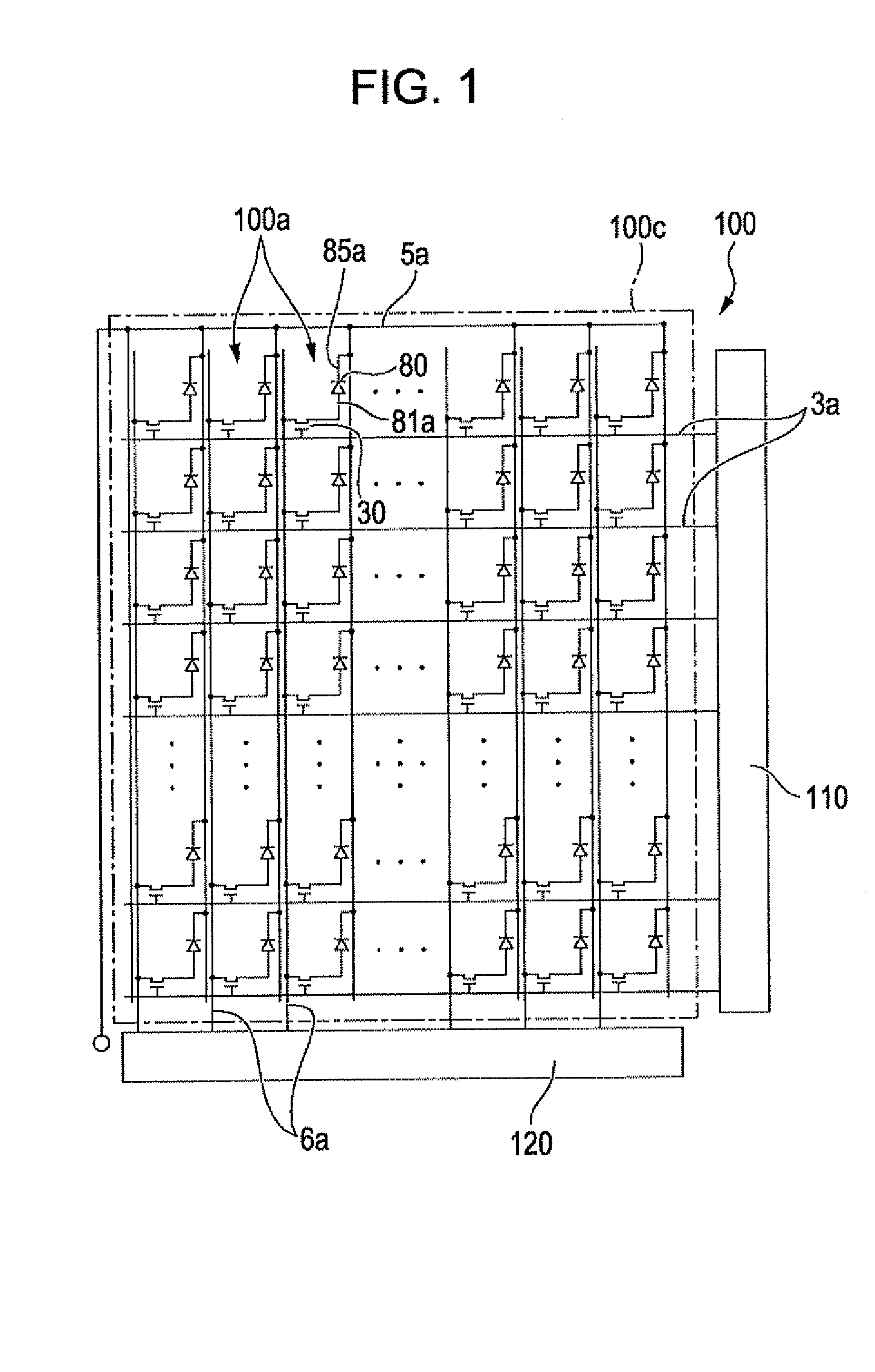
- Application Information
AI Technical Summary
Benefits of technology
Problems solved by technology
Method used
Image

Examples
first embodiment
Structure
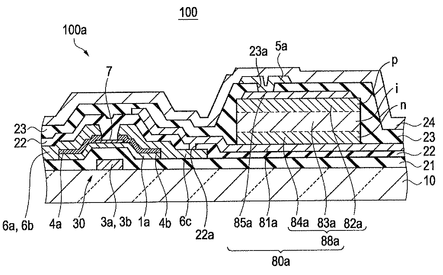
[0047]FIGS. 4A and 4B are a top plan view and a cross-sectional view of one of the pixels 100a of the solid-state image pickup device 100 according to a first embodiment of the invention, respectively, in which FIG. 4B is a cross-sectional view of the solid-state image pickup device 100 taken along the lines IVB-IVB in FIG. 4A. In FIG. 4A, the gate lines 3a and thin films or the like formed simultaneously with them are denoted by thin solid lines, the source lines 6a and thin films or the like formed simultaneously with them are denoted by dashed-dotted lines, semiconductor films (active layers) are denoted by thin and short dotted lines, the first electrode 81a of the photoelectric conversion element 80 is denoted by thin and long dotted lines, a semiconductor layer 88 of the photoelectric conversion element 80 is denoted by thick solid lines, and the second electrode 85a of the photoelectric conversion element 80 is denoted by thick and long dotted lines.
[0048]As illustra...
second embodiment
[0065]FIGS. 7A and 7B are a top plan view and a cross-sectional view of one of the pixels 100a of a solid-state image pickup device 100 according to a second embodiment of the invention, respectively, in which FIG. 7B is a cross-sectional view of the solid-state image pickup device 100 taken along the lines VIIB-VIIB in FIG. 7A. Since a basic structure of the present embodiment is the same as that of the first embodiment, the same or corresponding portions will be denoted by the same reference numerals, and redundant description thereof will be omitted.
[0066]In the solid-state image pickup device 100 illustrated in FIGS. 7A and 7B, similar to the first embodiment, the gate lines 3a and the source lines 6a extend in mutually intersecting directions on the substrate 10, and the pixel 100a is formed at each of the intersections of the gate lines 3a and the source lines 6a. Moreover, the bias line 5a extends to be parallel with the source lines 6a. Furthermore, in the present embodiment...
modified embodiment of second embodiment
[0073]FIGS. 8A and 8B are a top plan view and a cross-sectional view of one of the pixels 100a of a solid-state image pickup device 100 according to a modified embodiment of the second embodiment of the invention, respectively, in which FIG. 8B is a cross-sectional view of the solid-state image pickup device 100 taken along the lines VIIIB-VIIIB in FIG. 8A. Since a basic structure of the present embodiment is the same as that of the first and second embodiments, the same or corresponding portions will be denoted by the same reference numerals, and redundant description thereof will be omitted.
[0074]Although similar to the second embodiment, the solid-state image pickup device 100 illustrated in FIGS. 8A and 8B is an example in which the storage capacitor 90 is formed using the capacitance line to be electrically connected to be parallel with the photoelectric conversion element 80, in the present embodiment, the capacitance line 6e is formed simultaneously with the source line 6a. T...
PUM
 Abstract
Description
Claims
Application Information