Wire bonding method

a wire bonding and interconnection technology, applied in the direction of non-electric welding apparatus, manufacturing tools, welding apparatus, etc., can solve the problem of not being able to carry out direct bonding onto the interconnection

Inactive Publication Date: 2000-06-27
DENSO CORP
View PDF26 Cites 60 Cited by
  • Summary
  • Abstract
  • Description
  • Claims
  • Application Information

AI Technical Summary

Problems solved by technology

In this case, when the interconnection material is a material whose bondability with Au wire is poor, for example, Cu, Ni or flash Au plating, it is not possible to carry out direct bonding onto the interconnection.
However, providing this kind of substrate is not preferable in practice, and a method which makes it possible to carry out direct bo

Method used


Image

  • Wire bonding method
  • Wire bonding method
  • Wire bonding method

Examples


Embodiment Construction

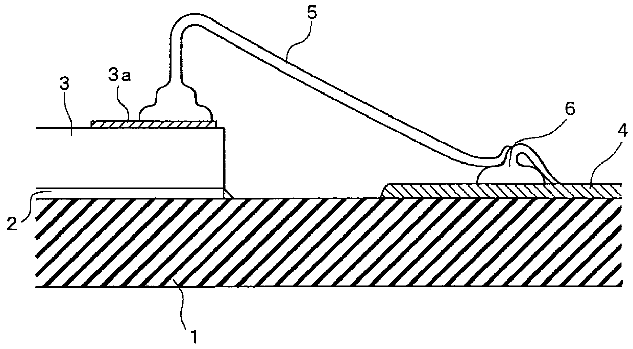
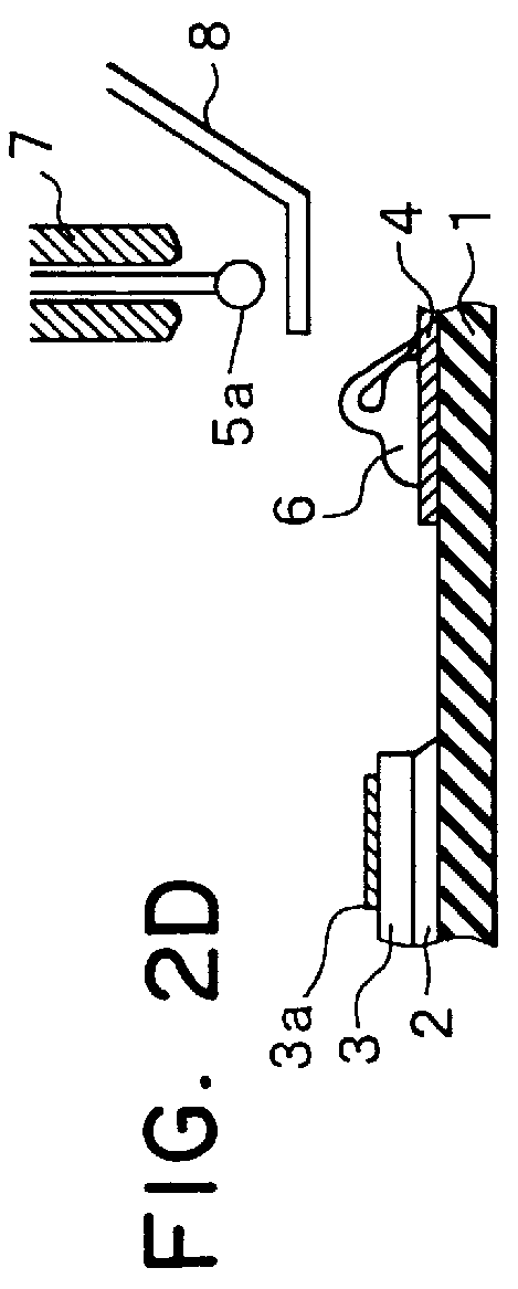
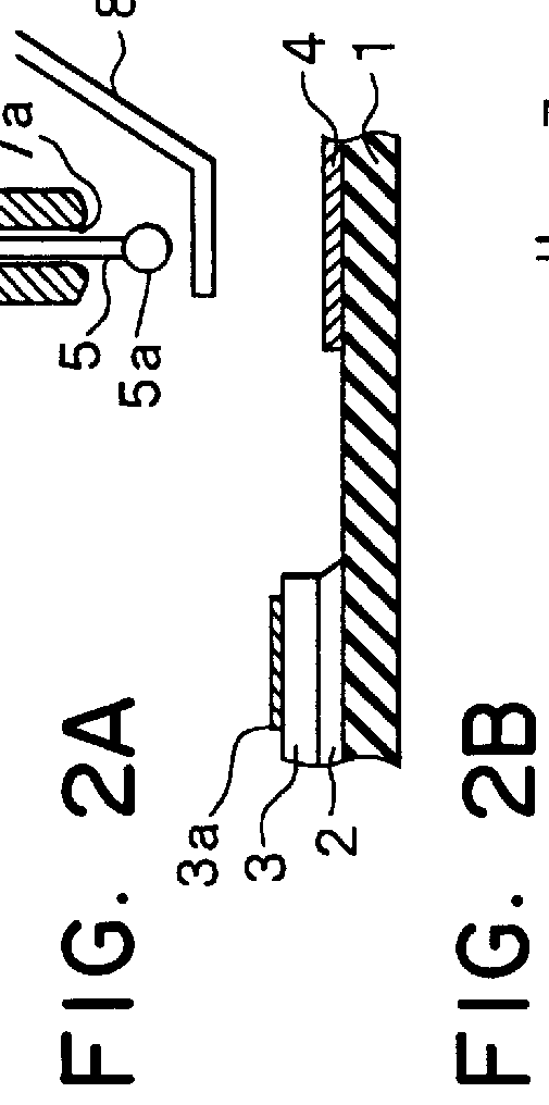
FIG. 1 shows a semiconductor chip and an interconnection wire-bonded together using a wire bonding method of an embodiment of the present invention.

A semiconductor chip 3 is die-mounted on a circuit board (a board such as a ceramic board or a printed board, or a lead frame) 1 by die-mounting paste 2. Also, an interconnection 4 made using an interconnection material, such as Cu, Ni, an interconnection conductor using Cu or Ni as a primary material (Cu thick film, Cu plating, Ni thick film, Ni plating and the like), or flash Au plating, whose bondability with an Au wire 5 is poor, is formed on the circuit board 1.

In this embodiment, when a bonding pad 3a of the semiconductor chip 3 and the interconnection 4 are to be wire-bonded using an Au wire 5, a bump 6 is formed in advance on the interconnection 4. After that, loop bonding is carried out between the bonding pad 3a of the semiconductor chip 3 and the bump 6.

A wire bonding method according to an embodiment of the present invention ...


PUM

PropertyMeasurementUnit
Capillary waveaaaaaaaaaa
Angleaaaaaaaaaa
Distanceaaaaaaaaaa

Abstract

A ball is formed at the tip of a wire projecting from a capillary. The capillary is positioned above an interconnection, and ball bonding forms a bump on the interconnection. The capillary is then moved next to the bump and wedge bonding is carried out. Next, the capillary is moved upward and another ball is formed at the tip of the wire, and the wire is primary bonded to a bonding pad of a semiconductor chip. The wire is then looped and the capillary is positioned above the bump, and secondary bonding is carried out. As a result, the formation of tails on the bump is prevented.

Description

This application is based upon and claims the benefit of priority of prior Japanese Patent Application No. H. 8-266372 filed on Oct. 7, 1996, the contents of which are incorporated herein by reference.1. Field of the InventionThis invention relates to a wire bonding method for carrying out wire bonding between two conductors.2. Related ArtTo carry out wire bonding between a semiconductor chip and an interconnection, a capillary having an Au wire passing through it is normally used. First, a ball is formed at the tip of the Au wire projecting from the capillary by electric discharge from a torch electrode, and then the capillary is positioned above the semiconductor chip and primary bonding is carried out. After that, the capillary is moved to above the interconnection and secondary bonding is carried out. The semiconductor chip and the interconnection are thereby wire bonded together.In this case, when the interconnection material is a material whose bondability with Au wire is poor...

Claims


Application Information

Patent Timeline
IPC IPC(8): B23K20/00H01L21/02H01L21/607H01L21/60
CPCB23K20/005H01L24/48H01L24/85H01L2924/01033H01L24/45H01L24/78H01L2224/32225H01L2224/45144H01L2224/48091H01L2224/48227H01L2224/48465H01L2224/4848H01L2224/48599H01L2224/49175H01L2224/73265H01L2224/78301H01L2224/85045H01L2224/85051H01L2224/85181H01L2224/85205H01L2224/85444H01L2224/85447H01L2224/85455H01L2224/85951H01L2224/85986H01L2224/92247H01L2924/01004H01L2924/01005H01L2924/01006H01L2924/01028H01L2924/01029H01L2924/01047H01L2924/01078H01L2924/01079H01L2924/01082B23K2201/40H01L2924/00014H01L2924/00H01L2924/00012B23K2101/40H01L2224/45015H01L2924/15787H01L2224/48644H01L2224/48647H01L2224/48655H01L24/73H01L24/49H01L2924/00015
Inventor MAEDA, YUKIHIRONAGASAKA, TAKASHISUZUKI, TOSHIO
Owner DENSO CORP
Why Eureka
Try Eureka