

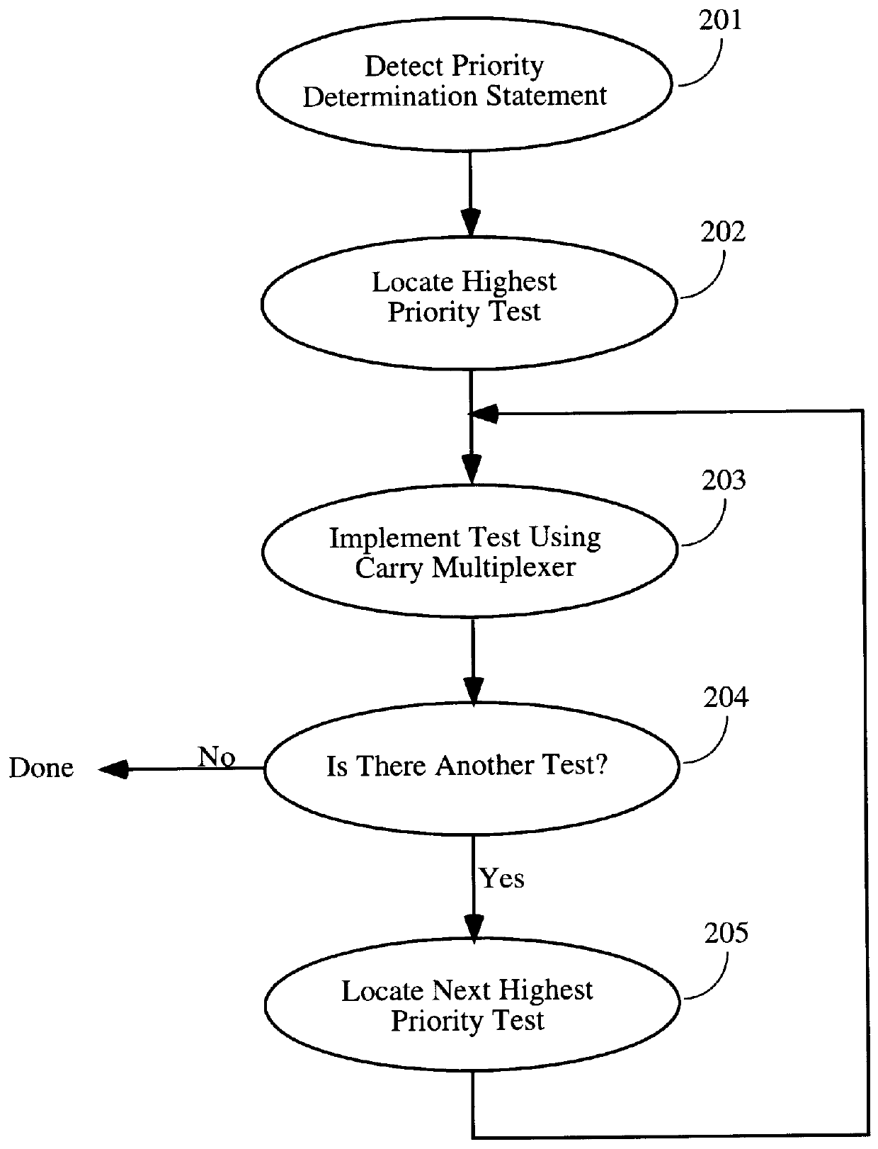
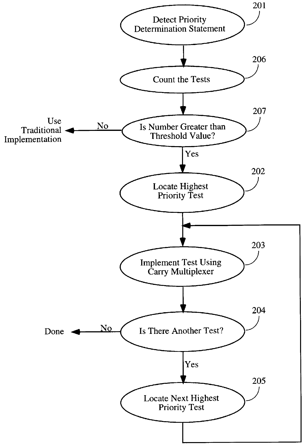
Method for implementing priority encoders using FPGA carry logic
- Summary
- Abstract
- Description
- Claims
- Application Information
AI Technical Summary
Problems solved by technology
Method used
Image

Examples
first embodiment
FIG. 4 shows how the priority encoder of FIG. 1 is implemented in the circuit of FIG. 3, according to the invention. This priority encoder requires 16 copies of the circuit of FIG. 3, one per test in the HDL code of FIG. 1. The circuits are labeled C0, C1, . . . , C14, C15. (Only four circuits are shown in FIG. 4, in order to simplify the drawing.)
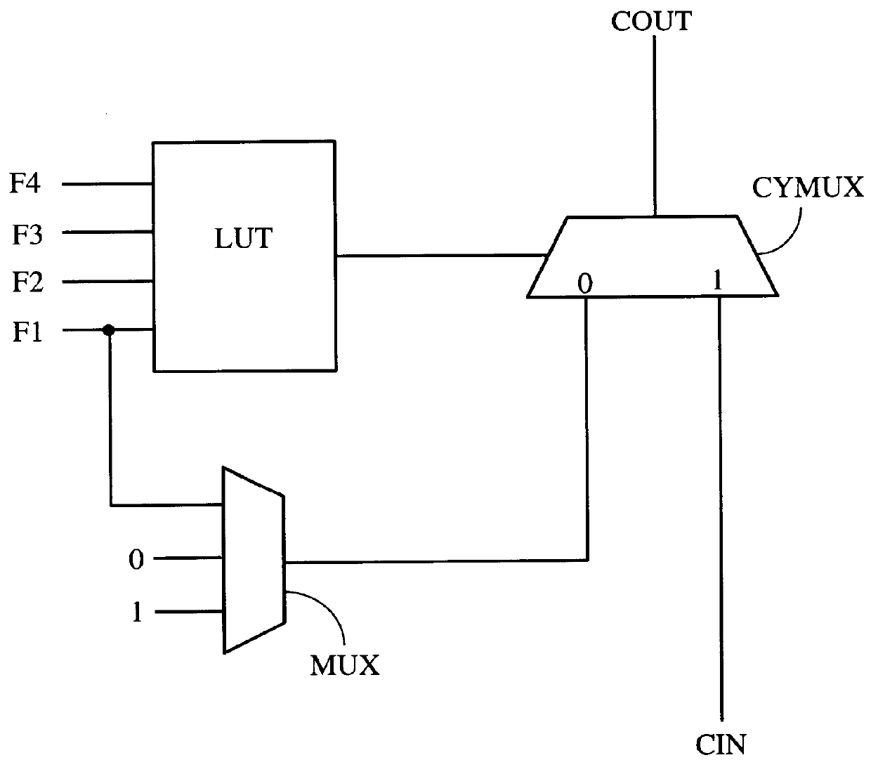
In FIG. 4, the output signal for the priority encoder is carried on line "dout". Line "dout" is driven by carry multiplexer CYMUXO in circuit C0, which circuit implements the first test. Input line din drives multiplexer MUX0, which is programmed to provide the signal on line din to the "0" input terminal of multiplexer CYMUX0. The "OR" function described in line 9 of FIG. 1 is implemented by lookup table LUT0, which is programmed as a 2-input NOR function with lines a and b providing the input signals. (Square brackets in HDL signal names are typically replaced by left and right arrows when the HDL code is compiled to form a circuit. Ther...
second embodiment
Detailed Description of a Second Embodiment
FIG. 5 shows a simplified portion of a CLB from the Xilinx XC4000E FPGA. The XC4000 CLB is described in detail in pages 4-11 through 4-23 of the Xilinx 1996 Data Book entitled "The Programmable Logic Data Book" (hereinafter referred to as "the Xilinx Data Book"), published September, 1996, available from Xilinx, Inc., 2100 Logic Drive, San Jose, Calif. 95124, which pages are incorporated herein by reference. (Xilinx, Inc., owner of the copyright, has no objection to copying these and other pages referenced herein but otherwise reserves all copyright rights whatsoever.) In this FPGA architecture, a single CLB includes one of the circuits shown in FIG. 5, as well as other logic. Each XC4000E CLB has two LUTs, and the circuit of FIG. 5 shows the carry logic associated with the two LUTs. FIG. 5 shows some portions of the XC4000E carry logic already programmed to pass signals through gates and multiplexers. More detailed diagrams of the XC4000E ...
third embodiment
Detailed Description of a Third Embodiment
FIG. 7 shows a simplified portion of a CLB from the Xilinx XC5200.TM. FPGA. The XC5200 CLB is described in detail in pages 4-184 through 4-190 of the Xilinx Data Book, which pages are incorporated herein by reference. In this FPGA architecture, a single CLB includes four of the circuits shown in FIG. 7, as well as other logic. However, the circuit in FIG. 7 is treated as an independent entity for the purposes of this example. The circuit of FIG. 7 includes a carry multiplexer CYM having a "1" input terminal coupled to carry input line CIN, a "0" input terminal coupled to input line FB, a carry output terminal coupled to carry output line COUT, and a carry select terminal coupled to the output terminal of lookup table LT. Lookup table LT is driven by input lines F1, F2, F3, and F4. Carry output line COUT is coupled to carry input line CIN of another copy of this circuit placed above FIG. 7. Carry input line CIN is coupled to carry output line...
PUM
 Abstract
Description
Claims
Application Information