Method to perform selective drain engineering with a non-critical mask

a selective drain and mask technology, applied in the direction of semiconductor devices, electrical equipment, transistors, etc., can solve the problems of reducing device performance, objectionable uncontrolled device asymmetry, and unable to achieve the desired effect, and neither of these options, however, are particularly desirabl

Inactive Publication Date: 2000-07-04
IBM CORP
View PDF23 Cites 50 Cited by
  • Summary
  • Abstract
  • Description
  • Claims
  • Application Information

AI Technical Summary

Benefits of technology

The present invention also includes the asymmetrical semiconductor devices produced according to the method of the invention. Most typically, this will include a field effect transistor, having an LDD on the drain side of the gate, but not on the source side of the gate, or having a halo on the source side of the gate, but not on the drain side of the gate, or both.

Problems solved by technology

Further, uncontrolled device asymmetry is objectionable and for these reasons, devices produced by angled ion implantation are generally made symmetric by rotating the semiconductor to allow the angled implant beam to implant from all sides of the gate.
The addition of an LDD region degrades device performance through increased series resistance and overlap capacitance.
Neither of these options, however, is particularly desirable.
Orienting all of the devices in the same direction significantly limits layout flexibility.
Obtaining such critical alignment is an expensive and error-prone procedure.
The same problem is encountered when constructing a halo implant only on the source side of the device.

Method used


Image

  • Method to perform selective drain engineering with a non-critical mask
  • Method to perform selective drain engineering with a non-critical mask
  • Method to perform selective drain engineering with a non-critical mask

Examples


Embodiment Construction

)

In describing the preferred embodiment of the present invention, reference will be made herein to FIGS. 1-4 of the drawings in which like numerals refer to like features of the invention.

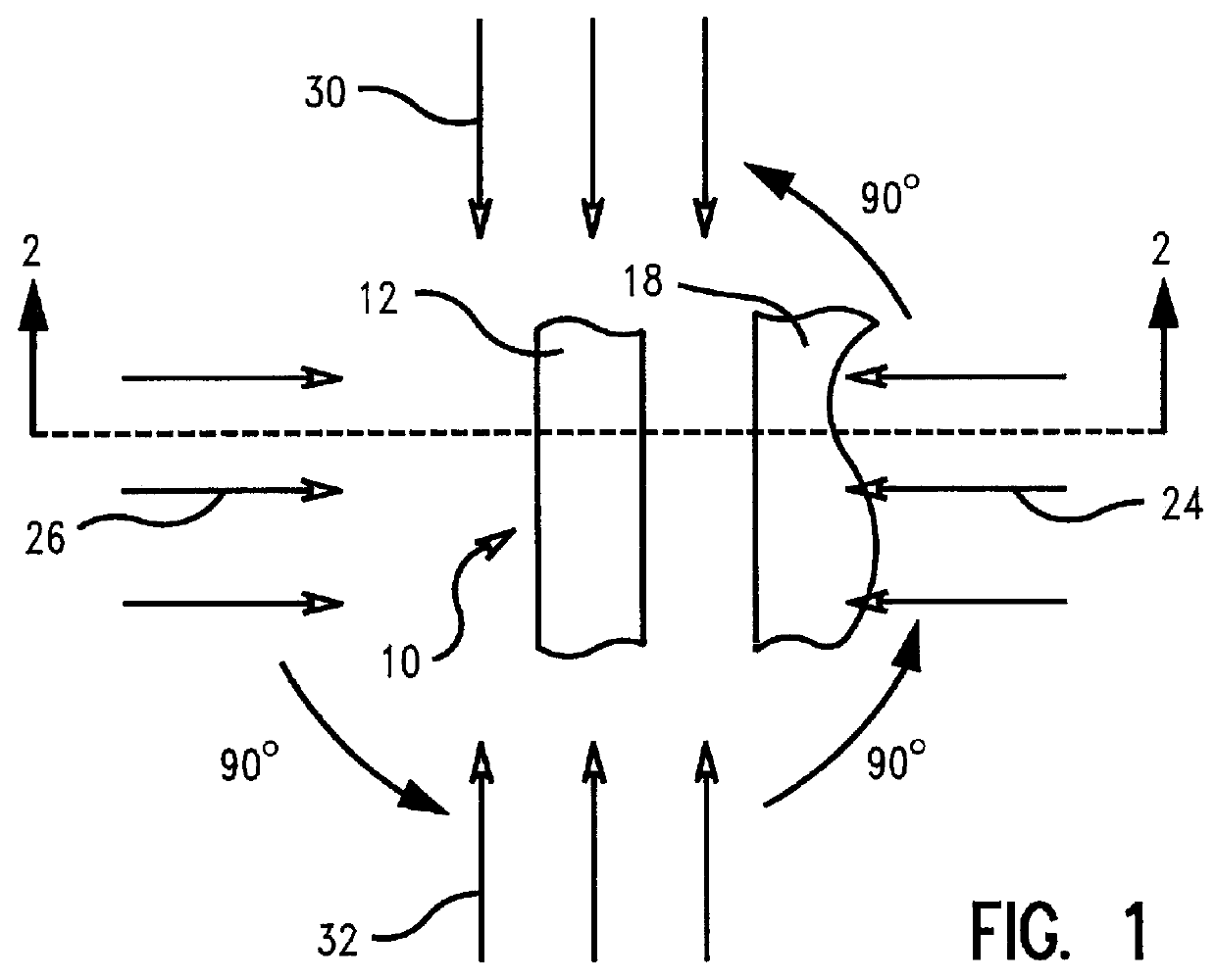
FIG. 1 provides a top plan view of a semiconductor device under construction in accordance with the present invention. A semiconductor surface 10 has a structure 12, such as the gate of a field effect transistor positioned upon it. As indicated by the cutaway at the ends of the gate 12, the gate may extend for some distance. Additional transistors will usually be positioned in an array around the transistor illustrated, and these transistors may be in any orientation relative to the transistor shown. In most implementations, however, the additional transistors will only be in one of four possible orthogonal orientations.

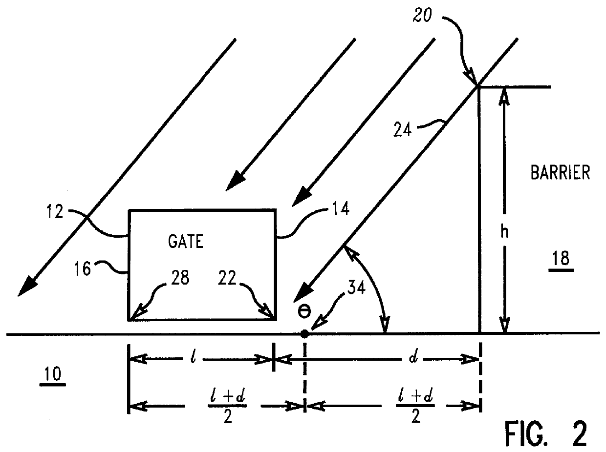
Referring to FIG. 2 which shows the gate 12 in cross section, it can be seen that the gate has a first side 14 and an opposite second side 16, separated by a gate width 1. Positione...


PUM


Abstract

A method of producing an asymmetrical semiconductor device with ion implantation techniques and semiconductor devices constructed according to this method in which a barrier of ion absorbing material of height h is positioned beside a structure on a semiconductor surface. The barrier is located at a maximum distance d from one side of the structure, and an angled ion implant is directed at the side of the structure. The maximum distance d of the barrier from the side of the structure is equal to the height of the barrier h divided by the tangent of the angle of the ion implant so that the side of the structure is shadowed from the ion implant. A second ion implant is directed to the opposite side of the structure on the semiconductor surface, thereby forming a desired implant and producing the asymmetrical semiconductor device.

Description

1. Field of the InventionThis invention relates to a method of producing an asymmetrical semiconductor device using angled ion implantation techniques. More specifically, this invention relates to a method of placing shallow ion implants under one side of a structure on a semiconductor surface, such as the gate of a field effect transistor.2. Description of Related ArtSemiconductor devices, such as metal oxide semiconductor field effect transistors (MOSFETs), produced with angled ion implantation techniques are often constructed symmetrically. This allows great flexibility in the layout of multiple devices as the source and drain are interchangeable (and both sides of the gate are consequently referred to simply as the "source / drain").For some applications, this type of device symmetry is highly desirable or essential. Further, uncontrolled device asymmetry is objectionable and for these reasons, devices produced by angled ion implantation are generally made symmetric by rotating th...

Claims


Application Information

Patent Timeline
Patent Type & Authority Patents(United States)
IPC IPC(8): H01L21/265H01L29/66H01L21/02H01L21/336H01L29/78H01L29/02H01L29/10
CPCH01L21/26586H01L29/1083H01L29/66659H01L29/7835H01L29/6659
Inventor HOOK, TERENCE B.HOYNIAK, DENNISNOWAK, EDWARD J.
Owner IBM CORP
Why Eureka
Try Eureka