Testing semiconductor devices for data retention

a technology of data retention and semiconductor devices, applied in the field of semiconductor devices, can solve the problems of reducing the quality of silicon oxide used, deteriorating data storage ability, and not being able to life-test the device or even test the device before delivery to customers

Inactive Publication Date: 2000-07-18
AVAGO TECH INT SALES PTE LTD
View PDF10 Cites 38 Cited by
  • Summary
  • Abstract
  • Description
  • Claims
  • Application Information

AI Technical Summary

Problems solved by technology

In a manufacturing process for devices of this type, many factors can lead to reduction of the quality of the silicon oxide used to isolate the floating gates, and thus lead to deterioration of the data storage ability over time.
But since the specified data retention periods are measured in years, it is not possible to life-test the devices or even samples of the devices before delivery to customers.
The amount of charge lost from the floating gates is of course dependent on time and temperature, but the temperature cannot be higher than certain limits or the devices are destroyed.
Increasing the time to a point where a reliable test is obtained i

Method used


Image

  • Testing semiconductor devices for data retention
  • Testing semiconductor devices for data retention
  • Testing semiconductor devices for data retention

Examples


Embodiment Construction

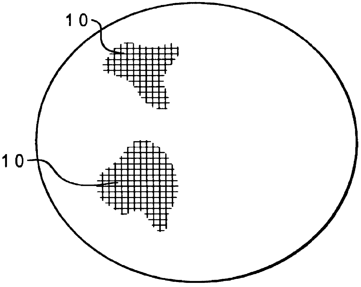
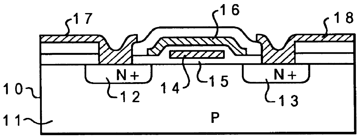
Referring to FIG. 1, an EEPROM device 10 is shown which may be subjected to the retention screening of the invention. Of course, this is merely a typical device structure, and forms no part of the method of the invention. The device includes a P-type silicon substrate 11 with N+ source and drain regions 12 and 13 formed therein. A polysilicon floating gate 14 is formed over the channel between source and drain, and is isolated from the channel by gate oxide 15. A polysilicon control gate 16 overlies the floating gate 14. An erase gate (which may take various forms) is positioned near the floating gate but is isolated from it by oxide. The erase gate is electrically connected to an external electrode by some path, whereas the floating gate is totally isolated. The source and drain regions 12 and 13 are connected by metal contacts 17 and 18 to operating bias and signal connections for operation and testing.

Only one memory cell is shown in FIG. 1 for purposes of explanation, but of cou...


PUM


Abstract

A method of screening EEPROMs for data retention quality employs a UV source which is arranged to be impinged upon the devices while in wafer form, at or near an electrical probe station. Known data is stored in memory cells on an EEPROM chip while the chip is in wafer form, at a probe station. The wafer is then moved beneath a UV silo near the probe station and exposed to UV light, for a period of time and at an intensity which is sufficient to cause leakage of charge from potentially leaky floating gates. The wafer is again subjected to electrical probe where the amount of change in retained charge is detected. From this test, an indication of the charge retention ability of the devices is obtained. The UV light increases the energy state of the stored charge thus accelerating the decay of the stored charge located on the floating gates in the EEPROM device. Bits that have inherent leakage paths decay more rapidly.

Description

1. Technical FieldThis invention relates to semiconductor devices, and more particularly to a method for testing programmable memory devices for data retention characteristics.2. Description of the Related ArtElectrically-erasable, programmable read-only memory devices (EEPROMs) operate on the basis of storing charge on a floating gate. The gate is floating in that it is not connected to any other electrode or to the silicon substrate, but instead is isolated from any conducting path by silicon oxide. The ability of the floating gate to store charge without leakage determines the ability of the EEPROM device to store data over a long period of time. Preferably, an EEPROM device can store data for many years.In a manufacturing process for devices of this type, many factors can lead to reduction of the quality of the silicon oxide used to isolate the floating gates, and thus lead to deterioration of the data storage ability over time. The devices must be tested at the end of the manuf...

Claims


Application Information

Patent Timeline
IPC IPC(8): G11C29/50G11C29/04
CPCG11C29/50G11C29/50016G11C16/04G11C2029/5002
Inventor HAEHN, STEVEN L.YAKURA, JAMES P.
Owner AVAGO TECH INT SALES PTE LTD
Why Eureka
Try Eureka