Unbalance-to-balance converter utilizing a transistor
a technology of unbalance-to-balance converter and transistor, which is applied in the direction of pulse generator, pulse manipulation, pulse technique, etc., can solve the problems of local oscillator signals, mixer input signals that leak power, and the phenomenon grows with an increase in the frequency of input signals
- Summary
- Abstract
- Description
- Claims
- Application Information
AI Technical Summary
Problems solved by technology
Method used
Image
Examples
embodiment 1
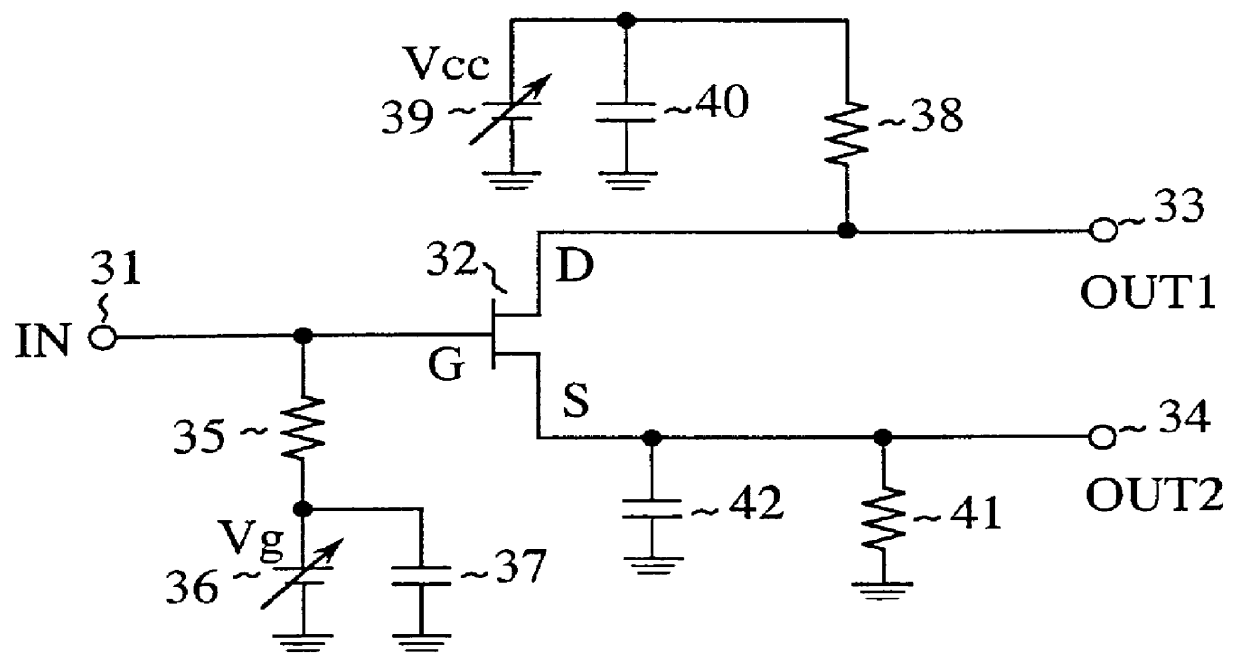
FIG. 1 is a circuit diagram showing an unbalance-to-balance converter in accordance with the present invention. In FIG. 1, the reference numeral 31 designates an input terminal 31 for inputting an unbalanced high frequency signal; 32 designates an FET that outputs, when the unbalanced high frequency signal is supplied to its gate terminal, a pair of balanced high frequency signals from its drain terminal and source terminal; 33 and 34 each designate an output terminal for producing one of the balanced high frequency signals; 35 designates a resistor with its first end connected to the gate terminal of the FET 32 and its second end connected to a power supply 36 that supplies a DC voltage; 37 designate a capacitor; 38 designates a resistor with its first end connected to the drain terminal of the FET 32 and its second end connected to a power supply 39 for supplying a DC voltage to the drain of the FET 32; 40 designates a capacitor; 41 designates a resistor with its first end connect...
embodiment 2
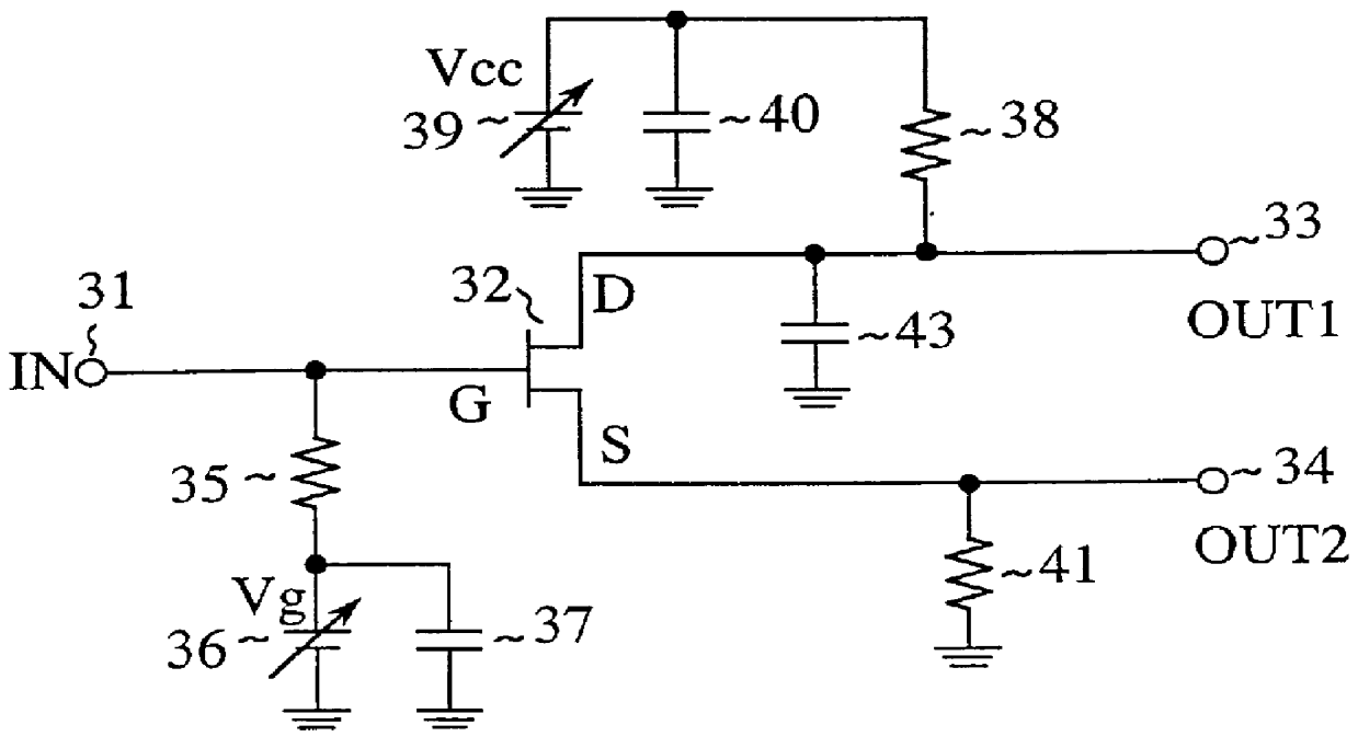
Although the foregoing embodiment 1 handles the case where the FET 32 is used in which the drain side parasitic capacitance Cpd is greater than the source side parasitic capacitance Cps, the FET 32 can also be used whose source side parasitic capacitance Cps is greater than the drain side parasitic capacitance Cpd. This can be implemented as shown in FIG. 2 by connecting between the drain terminal and the earth conductor a balanced output adjusting capacitor 43 having a capacitance equal to the capacitance difference Cps-Cpd between the source side parasitic capacitance Cps and drain side parasitic capacitance Cpd.
According to the present embodiment 2, the capacitance difference Cps-Cpd between the source side parasitic capacitance Cps and drain side parasitic capacitance Cpd is canceled, resulting in closely matched amplitude and almost complete opposition of the high frequency signals output from the drain terminal and source terminal.
embodiment 3
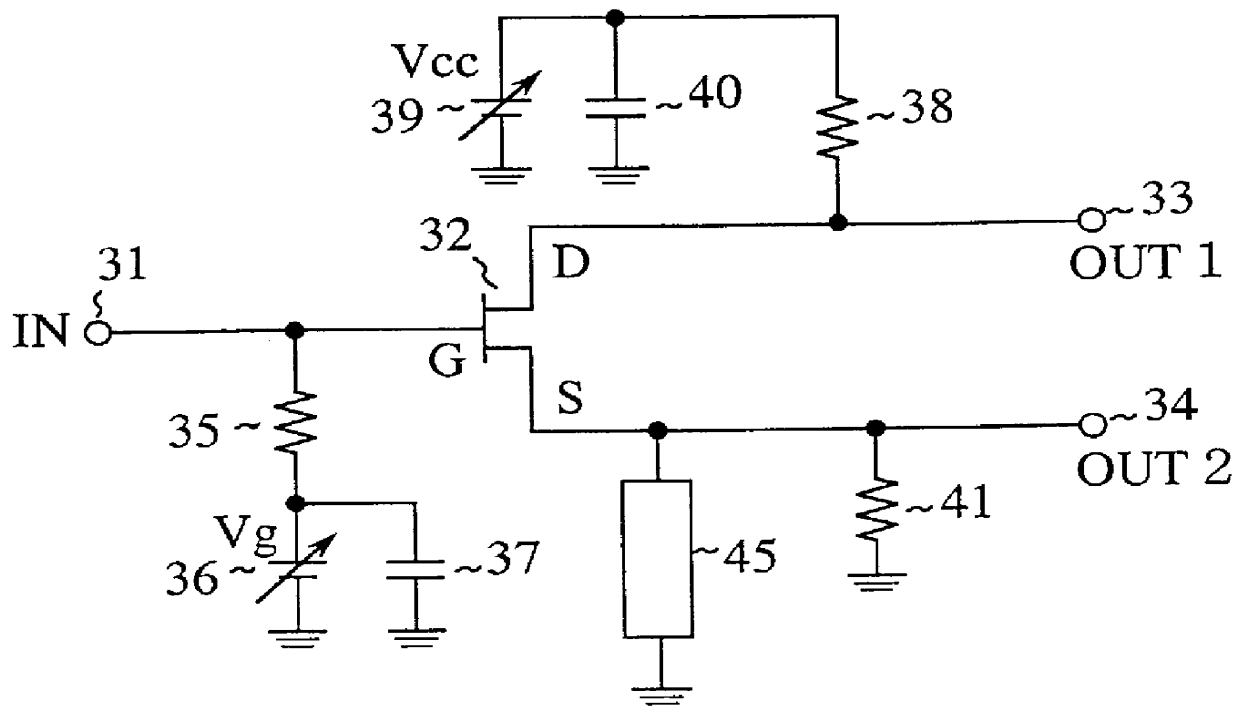
Although the balanced output adjusting capacitor 42 is connected between the source terminal and the earth conductor, and the balanced output adjusting capacitor 43 is connected between the drain terminal and the earth conductor in the foregoing embodiments 1 and 2, respectively, the balanced output adjusting capacitors 42 and 43 can be each replaced with an inter-digital capacitor.
More specifically, when the FET 32 is used whose drain side parasitic capacitance Cpd is greater than the source side parasitic capacitance Cps, an inter-digital capacitor 44 is connected between the source terminal and the earth conductor as shown in FIG. 3, but when the FET 32 is used whose source side parasitic capacitance Cps is greater than the drain side parasitic capacitance Cpd, the inter-digital capacitor 44 is connected between the drain terminal and the earth conductor. Since the inter-digital capacitor 44 consists of a coupling capacitance between two closely disposed conductive patterns, the ...
PUM
 Abstract
Description
Claims
Application Information


