Calibratable programmable phase shifter

a phase shifter and programmable technology, applied in the field of programmable phase shifters, can solve the problems of power supply noise, power supply noise, phase shift deviation from the desired linear function,

Inactive Publication Date: 2000-08-15
CREDENCE SYSTEMS
View PDF3 Cites 57 Cited by
  • Summary
  • Abstract
  • Description
  • Claims
  • Application Information

AI Technical Summary

Problems solved by technology

The phase angle is controlled by 10-bit input control data N. Ideally phase shifter 10 should provide a phase shift between T.sub.0 and T.sub.OUT that is a linear function of the value of input control data N. However, as explained below, phase shifter 10 has inherent sources of error that cause the phase shift to deviate from the desired linear function of the value of N.
One major source of error is power supply noise.
In synchronous circuits using T.sub.0 as the primarily reference clock for synchronous operations, the largest component of power supply noise typically comes from the T.sub.0 signal.

Method used


Image

  • Calibratable programmable phase shifter
  • Calibratable programmable phase shifter
  • Calibratable programmable phase shifter

Examples


first embodiment

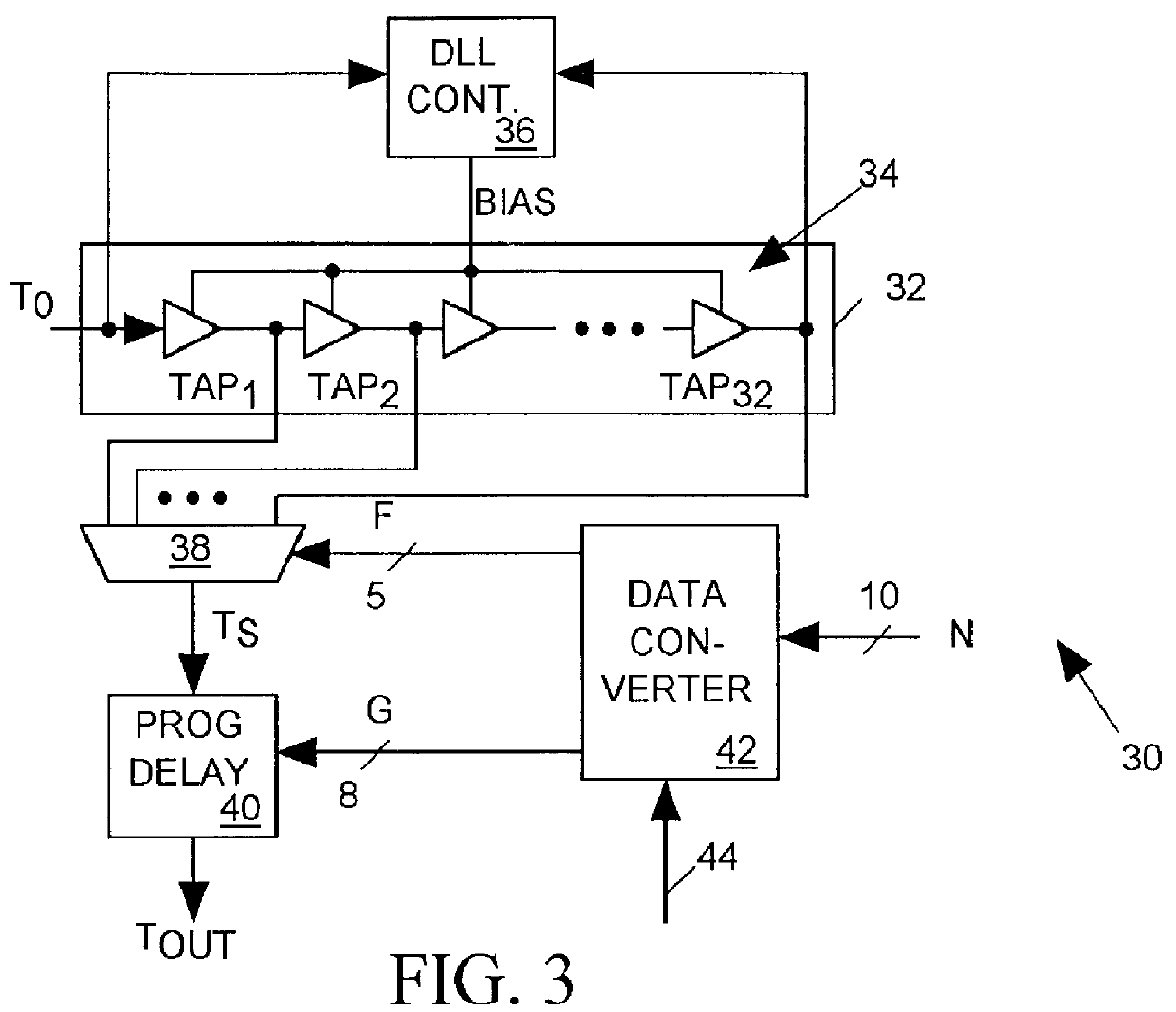
FIG. 4 illustrates data converter 42 of FIG. 3, a random access memory (RAM) 46 addressed by input data N and reading out F and G. During calibration, a value of (F,G) for each value of input N is written into address N of RAM 46 via bus 44. The phase shift provided for each value of N is then measured and the value of the (F,G) data stored in the corresponding RAM 46 address N is incrementally increased or decreased depending on whether the measured phase shift is too small or too large. The process is repeated until a value of (F,G) providing the closest approximation of a linear relationship between the value of N and phase shift is stored at each RAM 46 address.

second embodiment

The embodiment of data converter 42 illustrated in FIG. 4 allows complete freedom in choosing a tap signal and a programmable delay for each value of N. However since RAM 46 must provide 2.sup.10 M-bit storage locations, RAM 46 must be very large. FIG. 5 illustrates data converter 42 of FIG. 3 in which the upper five bits of the 10-bit input data N directly provide the five F bits controlling multiplexer 38 of FIG. 3 while a RAM 48 addressed by the 10-bit N data provides only the 8-bit control data input G to programmable delay circuit 40. RAM 48 of FIG. 5, while still requiring 2.sup.10 storage locations, is none the less smaller than RAM 46 of FIG. 4 because it stores only eighth bits instead of thirteen bits at each storage location. Although the embodiment of FIG. 5 does not allow for adjustment of tap selection for each value of N, when the variation in delay provided by each delay element 34 is small enough, it is not necessary for tap selection to be an adjustable function of...

third embodiment

FIG. 6 illustrates data converter 42 of FIG. 3 in which the upper five bits NH of the 10-bit input data N directly provide the 5-bit F data value controlling multiplexer 38 of FIG. 3 and also address a RAM 58 write accessed by bus 44. RAM 58 stores and reads out 7-bit "delay correction" data B when addressed by the NH bits. A scaling unit 60 converts the lower five bits NL of the input N data to 8-bit delay control data A. An adder 62 sums the delay control data A with the delay correction data B to produce the 8-bit control data G provided to programmable delay circuit 40 of FIG. 3.

The value of the five NL bits can range from 0 to 2.sup.5 -1 and the value of seven delay correction data B can range from 0 to 2.sup.7 -1. Scaling unit 60, which may be implemented for example by dedicated logic or a ROM, suitably provides the relation

A=(2.sup.8 -2.sup.7)NL / (2.sup.5 -1)

Thus the value of A can range from 0 to 2.sup.8 -2.sup.7 and the value of G can range from 0 to 2.sup.8 -1. When the ta...


PUM


Abstract

A programmable phase shifter includes a tapped delay line for successively delaying a periodic reference signal to produce a set of phase distributed tap signals. A multiplexer selects one of the tap signals as input to a programmable delay circuit which further delays the selected tap signal to produce an output signal that is phase shifted from the reference signal. A programmable data converter converts input data indicting a desired phase shift between the reference signal and the output signal into data for controlling the multiplexer selection and the amount of delay provided by the programmable delay circuit. The relationship between conversion table input and output data is adjusted so that the period of the output signal has a desired linear relationship to the input data value.

Description

1. Field of the InventionThe present invention relates in general to a programmable phase shifter for phase shifting a periodic input signal by an adjustable amount, and in particular to a programmable phase shifter that can be easily calibrated to provide a phase shift that is a linear function of the value of input control data.2. Description of Related ArtFIG. 1 illustrates a prior art programmable phase shifter 10 for phase shifting a periodic input signal T.sub.0 by an adjustable phase angle to produce an output signal T.sub.OUT. The phase angle is controlled by 10-bit input control data N. Ideally phase shifter 10 should provide a phase shift between T.sub.0 and T.sub.OUT that is a linear function of the value of input control data N. However, as explained below, phase shifter 10 has inherent sources of error that cause the phase shift to deviate from the desired linear function of the value of N.Phase shifter 10 includes a tapped delay line 12 formed by a set of delay element...

Claims


Application Information

Patent Timeline
Patent Type & Authority Patents(United States)
IPC IPC(8): H03H11/26H03H17/08
CPCH03H11/265H03H17/08
Inventor CHAPMAN, D. JAMESCURRIN, JEFFREY D.
Owner CREDENCE SYSTEMS
Why Eureka
Try Eureka