Method of integration of nitrogen bearing high K film

Inactive Publication Date: 2000-08-29
GLOBALFOUNDRIES INC
View PDF4 Cites 55 Cited by
  • Summary
  • Abstract
  • Description
  • Claims
  • Application Information

AI Technical Summary

Problems solved by technology

However, the scaling of silicon dioxide gate dielectric layers has introduced another set of problems.
To begin with, very thin silicon dioxide layers have been historically difficult to fabricate with a consistent thickness across a given wafer, from wafer to wafer and from lot to lot.
In addition, as the thickness of silicon dioxide is scaled downward, the potential for reliability problems associated with dielectric breakdown and hot and cold carrier injection degradation increases.
Hot and cold carrier degradation can significantly reduce device performance, while dielectric breakdown can lead to complete device failure.
One potential cause of carrier injection and potential dielectric breakdown is thought to occur as a result of interface traps near the Si--SiO.sub.2 interface.
Ind

Method used


Image

  • Method of integration of nitrogen bearing high K film
  • Method of integration of nitrogen bearing high K film
  • Method of integration of nitrogen bearing high K film

Examples


Embodiment Construction

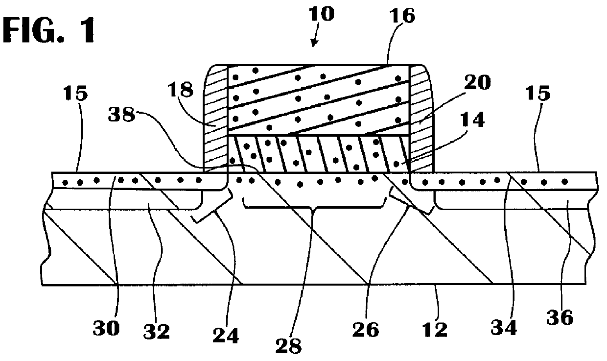
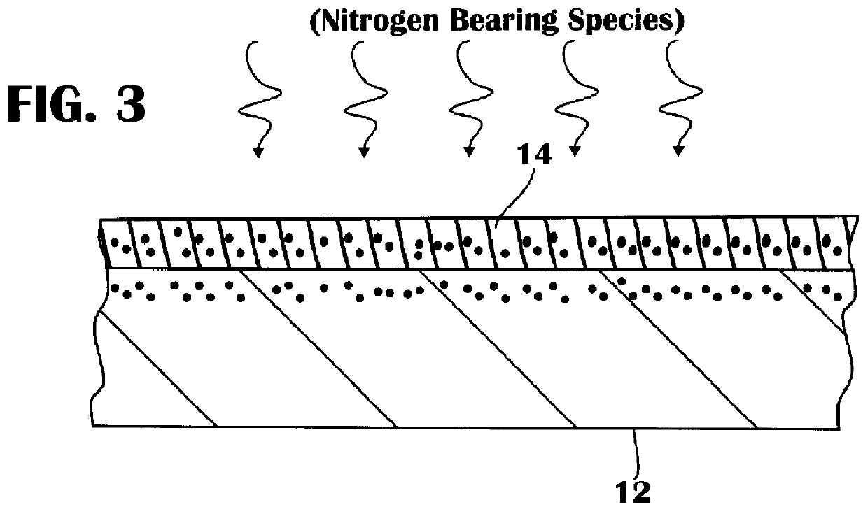
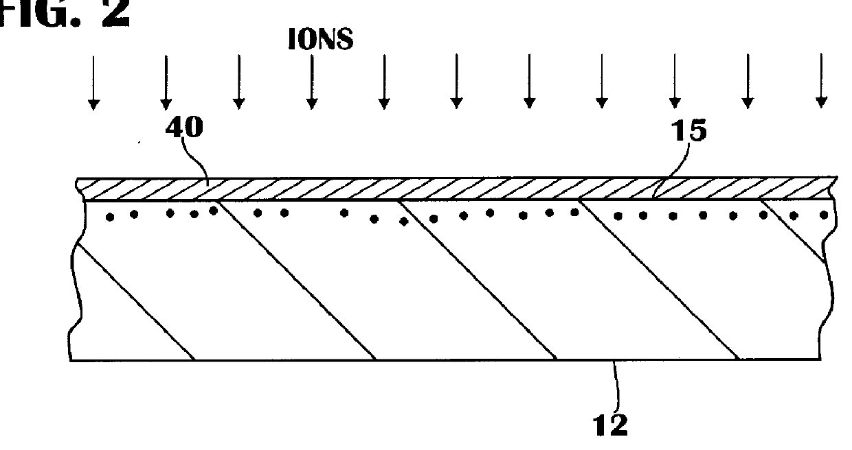
In the drawings described below, reference numerals are generally repeated where identical elements appear in more than one figure. Turning now to the drawings, and in particular to FIG. 1, there is shown a cross-sectional view of an exemplary embodiment of a transistor 10 that is formed on a semiconductor substrate 12. The semiconductor substrate 12 may be composed of n-doped, or p-doped silicon, silicon-on-insulator, or other suitable substrate materials. The transistor 10 includes an insulating or gate dielectric layer 14 that is formed on the upper surface 15 of the substrate 12 and a gate electrode 16 that is formed on the first insulating layer 14. Dielectric sidewall spacers 18 and 20 are positioned adjacent the gate dielectric layer 14 and the gate electrode 16. Source / drain regions 24 and 26 are formed in the substrate 12 and laterally separated to define a channel region 28 beneath the gate dielectric layer 14 and the gate electrode 16. The source / drain region 24 includes ...


PUM


Abstract

A transistor and a method of making the same are provided. The transistor includes a substrate that has an upper surface and a gate dielectric layer positioned on the substrate that has a first quantity of nitrogen therein. A gate electrode is positioned on the gate dielectric layer. First and second source/drain regions are positioned in the substrate and laterally separated to define a channel region beneath the gate dielectric layer. The gate dielectric layer may be composed of a high K material with a thin equivalent thickness of oxide, such as TiO2, Ta2O5, CrO2 or SrO2. The nitrogen suppresses later oxide formation which may otherwise increase the equivalent thickness of oxide of the gate dielectric layer. Nitrogen may also be incorporated into the substrate and the gate electrode.

Description

1. Field of the InventionThis invention relates generally to semiconductor processing, and more particularly, to a transistor with a gate dielectric layer that has a high dielectric constant and a level of nitrogen doping, and to a method of making the same.2. Description of the Related ArtA conventional field effect transistor implemented in silicon typically consists of a source and a drain formed in a silicon substrate, and separated laterally to define a channel region in the substrate. A gate dielectric layer is positioned on the substrate over the channel region and a gate electrode composed of a conducting material, such as aluminum or doped polysilicon, is disposed on the gate dielectric layer. The gate electrode is designed to emit an electric field into the channel region. Changes in the electric field emitted by the gate electrode enable, or alternatively, disable the flow of current between the source and the drain.In a conventional process flow for forming a typical fie...

Claims


Application Information

Patent Timeline
IPC IPC(8): H01L21/28H01L21/02H01L29/51H01L21/265H01L21/336H01L29/40H01L21/316
CPCH01L21/26506H01L21/28035H01L21/28185H01L21/28202H01L21/2822H01L29/518H01L29/6659H01L21/31604H01L21/31691H01L21/02186H01L21/02183H01L21/02192H01L21/02332H01L21/02337
Inventor GARDNER, MARK I.GILMER, MARK C.
Owner GLOBALFOUNDRIES INC
Why Eureka
Try Eureka