Semiconductor memory device

a memory chip and semiconductor technology, applied in the field of semiconductor memory chips, can solve problems such as coupling noise, memory chip performance degradation, and word line deformation

Inactive Publication Date: 2000-08-29
HYUNDAI ELECTRONICS IND CO LTD
View PDF10 Cites 41 Cited by
  • Summary
  • Abstract
  • Description
  • Claims
  • Application Information

AI Technical Summary

Problems solved by technology

First, in the row decoder section, the GWL signal and GWLb signal which control a plurality of sub word lines are generated by the row decoder and connected to four SWDs. This means that there are two metal lines, GWLb and GWL signal lines, every four polysilicon word line. This causes defects in the word line during the fabrication process due to shortage of design rule margin. Furthermore, coupling noise is generated between the word lines and between the word line and

Method used


Image

  • Semiconductor memory device
  • Semiconductor memory device
  • Semiconductor memory device

Examples


Embodiment Construction

Reference will now be made in detail to the preferred embodiments of the present invention, examples of which are illustrated in the accompanying drawings.

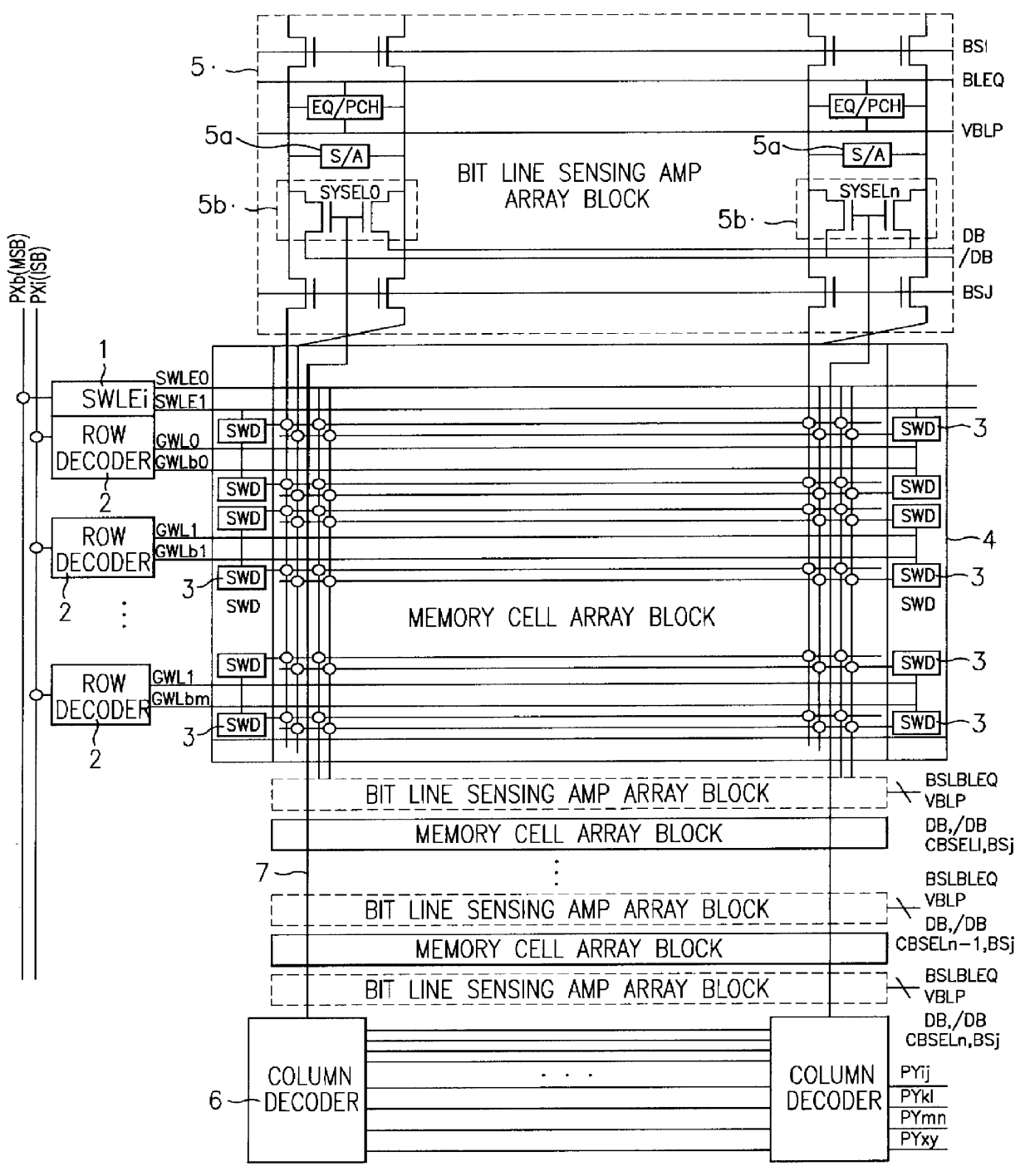
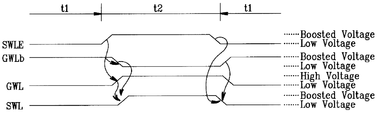
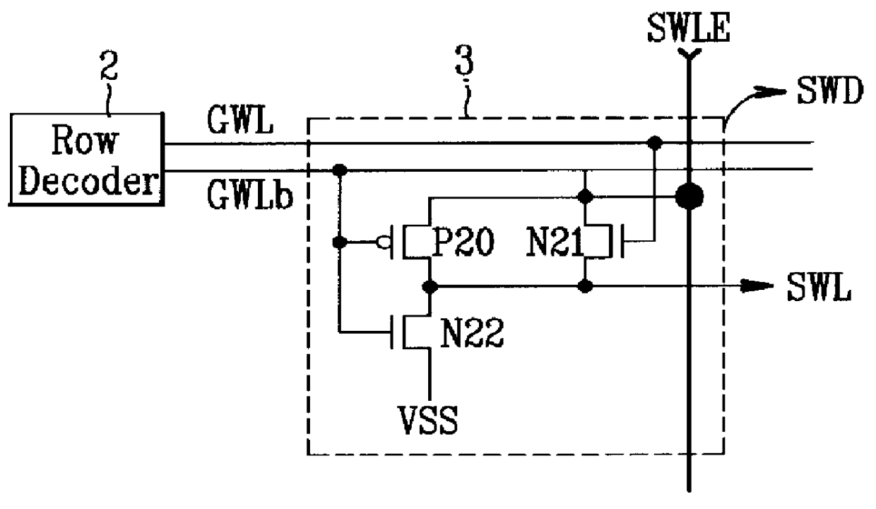
FIG. 4 is a schematic section diagram of a semiconductor memory device according to the present invention.

The semiconductor memory device of the present invention includes a plurality of memory cell arrays 44, a plurality of bit line sensing amplifier arrays 45 connected to each of the memory cell arrays 44, for sensing data of each memory cell array 44 through a bit line and bit bar line, a plurality of column decoders 46 for activating a column selection line 47 corresponding to an input address signal, a level shifting section 48 for controlling the level of the column selection line connected to the column decoder 46, a data input / output controlling section 49 for controlling a Y-gate 45b connected to the bit line and bit bar line so that the data output from the bit line sensing amplifier array 45 which is selected by the con...


PUM


Abstract

Disclose is a semiconductor memory device including a plurality of memory cell arrays, row and column decoders for selecting/driving each memory cell, and a plurality of bit line sensing amplifier arrays for sensing data of each memory cell, the semiconductor memory device comprising: a plurality of sub word line driver sections for driving each memory cell with a sub word line enable selection signal (SWLE) decoded by LSB address and with a global word line signal (GWLb) decoded by MSB address in the row decoder; a row decoding precharge signal generating section (RDPRi/VBFi) for applying a precharge signal to the row decoder and a voltage Vbb to the GWLb signal by means of the MSB address PXb; a level shifting section for shifting and transmitting an output signal from the column decoder to column selection lines which connects the column decoder with the bit line sensing amplifier array in series; and a data input/output controlling section for selectively applying an active signal to the bit line sensing amplifier array according to a level of the column selection line.

Description

1. Field of the InventionThe present invention relates to a semiconductor memory device and, more particularly, to a semiconductor memory device which drives a plurality of sub word line drivers using output signals (GWLB,SWLE) of a row decoder so as to efficiently control a column selection signal.2. Discussion of the Related ArtA related art semiconductor memory device will be described below with reference to the accompanying drawings.FIG. 1 shows the configuration of a related art semiconductor memory device.The related art semiconductor memory device, on the whole, includes a memory cell array, a row decoder and sub word line driver section, and a column selection driver section.The row decoder and sub word line driver section includes a plurality of sub word line driver (SWD) sections 3 for driving memory cells in memory cell array sections 4, a row decoder 2 for generating a plurality of global word line bar (GWLb) signals and global word line (GWL) signals in the SWD section...

Claims


Application Information

Patent Timeline
IPC IPC(8): G11C11/408G11C8/10G11C8/00G11C11/418G11C11/401G11C11/407
CPCG11C8/10G11C11/4087
Inventor KHANG, CHANG MANJUN, YOUNG HYUN
Owner HYUNDAI ELECTRONICS IND CO LTD
Why Eureka
Try Eureka