Electroluminescent display with constant current control circuits in scan electrode circuit

a control circuit and electrode circuit technology, applied in the field of electroluminescent displays, can solve the problems of increasing the time constant, affecting the heat generation of scan driver ics, and affecting the charging and discharging time of scan drivers, so as to reduce the charging and discharging time

Inactive Publication Date: 2000-09-19
DENSO CORP
View PDF26 Cites 92 Cited by
  • Summary
  • Abstract
  • Description
  • Claims
  • Application Information

AI Technical Summary

Benefits of technology

It is an object of the present invention to solve the problems associated with the generation of heat an...

Problems solved by technology

When the scan signal is applied, a problem arises in that the scan driver ICs are significantly affected by generation of heat because the values of the charge and discharge currents are very high.
Further, since a rush current flows at the time of charge and discharge, a problem arises in that the scan driver ICs are dama...

Method used


Image

  • Electroluminescent display with constant current control circuits in scan electrode circuit
  • Electroluminescent display with constant current control circuits in scan electrode circuit
  • Electroluminescent display with constant current control circuits in scan electrode circuit

Examples


second embodiment

the present invention will now be described.

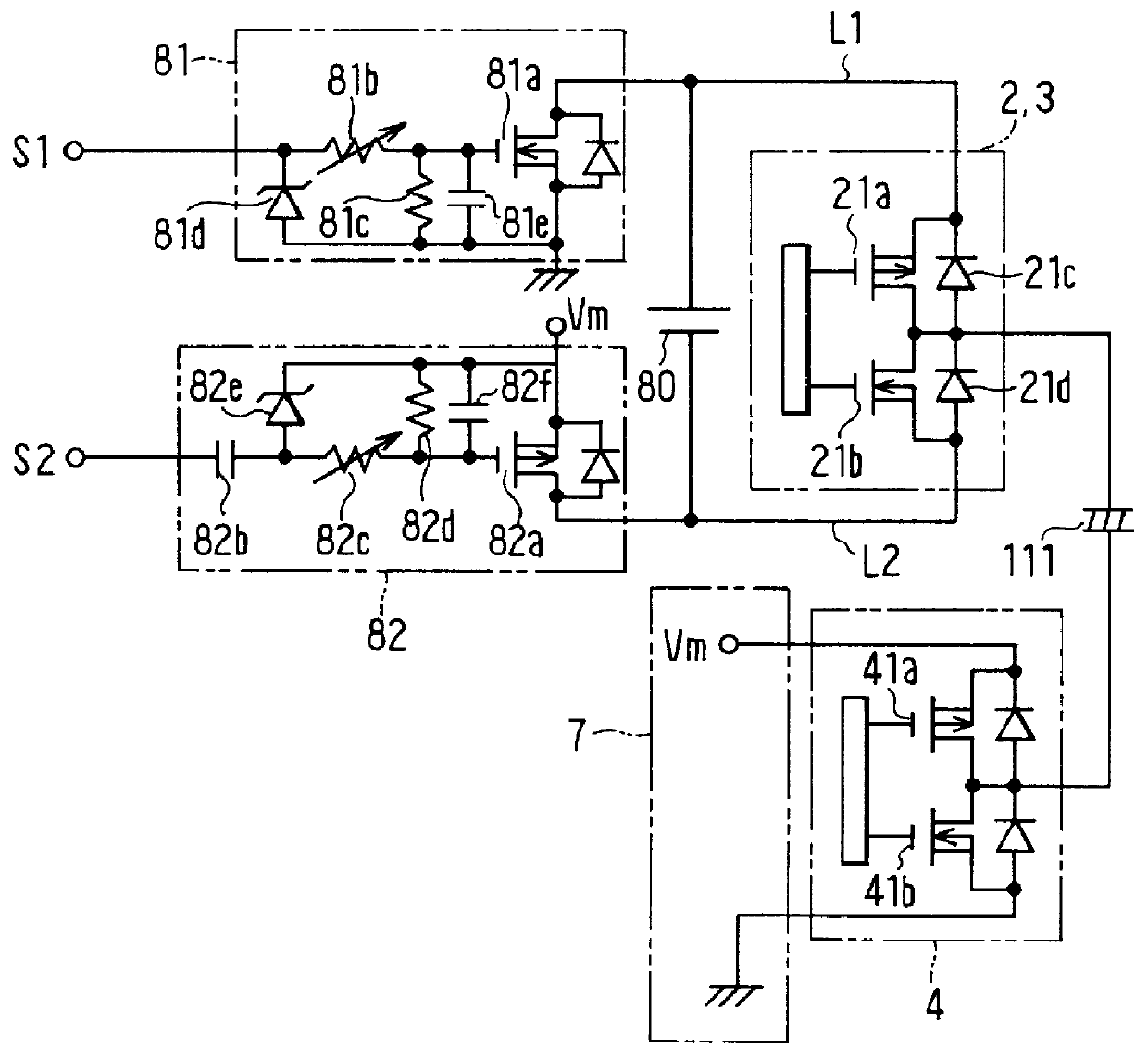
FIG. 5 shows another configuration of the constant current control circuits 81 and 82. In the configuration shown in FIG. 5, constant current control is performed by detecting the drain current. Specifically, variable resistors 81f and 82g are respectively inserted at the source side of the n-channel FET 81a and p-channel FET 82a of the constant current control circuits 81 and 82 to decrease the drain current as a result of a decrease in the gate-source voltage in response to an increase in the drain current and to conversely increase the drain current as a result of an increase in the gate-source voltage in response to a decrease in the drain current.

Thus, the drain currents of the n-channel FET 81a and p-channel FET 82a are controlled at constant currents.

The above-described variable resistors 81f and 82g for current detection will not increase the charge and discharge time to a problematic level because they can be implemented using par...

third embodiment

the present invention will now be described.

Although each of the constant current control circuit 81 and 82 performs both charging and discharging in the above embodiments, charging and discharging may be performed using separate constant current control circuits. FIG. 6 shows a configuration for such a case.

In the configuration shown in FIG. 6, four constant current control circuits 83 through 86 are provided. The constant current control circuits 83 and 84 have the same configuration as that of the constant current control circuits 81 and 82 in FIG. 4. The constant current control circuit 85 includes an n-channel FET 85a, a coupling capacitor 85b, a variable resistor 85c, a resistor 85d, a Zener diode 85e for protecting the input, and a capacitor 85f for removing noise. Similarly, the constant current control circuit 86 includes an p-channel FET 86a, a coupling capacitor 86b, a variable resistor 86c, a resistor 86d, a Zener diode 86e for protecting input, and a capacitor 86f for r...

fourth embodiment

the present invention will now be described.

When driving is performed with inverted fields, the voltage of the scan electrodes is kept at a desired reference voltage by performing precharging when field switching occurs. That is, the voltage equals the offset voltage Vm in the positive field and equals the ground voltage in the negative field.

An increase in the size of the EL display panel 1 increases the total capacity of the EL elements, which results in an increase in the time required for precharging if the scan signal supply circuits 5 and 6 are configured using constant current control circuits as in the various embodiments described above. As a result, when line sequential scanning is started before precharging is completed at the time field switching, the scan electrodes for which the precharging has not been completed will have a low scan voltage and hence low intensity. Therefore, variation in intensity occurs at the time of field switching, resulting in a problem in that ...


PUM


Abstract

To reduce the influence of generation of heat at scan driver ICs during the application of a scan signal with reduced time of charge and discharge and to eliminate the problem of a rush current, in an EL display where scan driver Ics sequentially apply a scan signal to a plurality of scan electrodes and data driver IC applies a data signal to data electrodes to selectively cause EL elements to emit light responsive to the scan signal and data signal, constant current control circuits are provided to control charge and discharge currents at constant currents during the application of the scan signal to the scan electrodes by the scan driver ICs.

Description

BACKGROUND OF THE INVENTION1. Field of the InventionThe present invention relates to an EL display for performing display by driving EL (electro-luminescence) elements for emission of light.2. Description of Related ArtConventional circuits for driving EL elements for emission of light include the one disclosed in Japanese Patent Publication Laid-Open No. Hei 5-333815. This circuit has an EL display panel on which a plurality of scan electrodes and a plurality of data electrodes are arranged in a matrix and EL elements formed in positions where the scan electrodes and data electrodes intersect with each other. Scan driver ICs sequentially apply a scan signal to the plurality of scan electrodes and data driver ICs apply a data signal to the data electrodes to selectively cause the plurality of EL elements to emit light responsive to the scan signal and data signal.In the above-described configuration, the scan driver ICs have FETs at their output stages, and charge and discharge curr...

Claims


Application Information

Patent Timeline
IPC IPC(8): G09G3/30
CPCG09G3/30G09G2300/06G09G2310/0248G09G2310/0256G09G2310/0267G09G2310/0275G09G2330/045G09G2330/06
Inventor NISHIOKA, KENKISHITA, HIROYUKIOSADA, MASAHIKO
Owner DENSO CORP
Why Eureka
Try Eureka