Voltage level shifting apparatuses and methods

a technology of voltage level and shifting apparatus, applied in the direction of logic circuit, pulse automatic control, pulse technique, etc., can solve the problems of adding additional circuitry and complexity, and achieve the effects of reducing delay, reducing circuit complexity, and reducing overall die siz

Active Publication Date: 2013-02-26
INTEGRATED DEVICE TECH INC
View PDF17 Cites 9 Cited by
  • Summary
  • Abstract
  • Description
  • Claims
  • Application Information

AI Technical Summary

Benefits of technology

[0010]Embodiments of the present invention include apparatuses and methods for voltage level shifting that reduce delays, reduce circuit complexity, reduce overall die size, or combinations thereof.
[0015]Other embodiments of the present invention relate to methods for shifting an input voltage level to a different output voltage level. The method includes turning off a first n-channel transistor operably coupled between a low potential and an output signal. The output signal is charged from the low potential to a higher supply voltage by turning on a first p-channel transistor operably coupled between the higher supply voltage and the output signal. The method also includes turning off a second p-channel transistor operably coupled between the higher supply voltage and the output signal. An inverted output signal is discharged from the higher supply voltage to the lower potential by turning on a second n-channel transistor operably coupled between the low potential and the inverted output signal. A discharging time of the inverted output signal is reduced by maintaining a gate-side node of a second gate-to-drain capacitor of the second n-channel transistor at a lower supply voltage.

Problems solved by technology

However, most proposals add additional circuitry and complexity in an effort reduce power or reduce propagation delays.

Method used


Image

  • Voltage level shifting apparatuses and methods
  • Voltage level shifting apparatuses and methods
  • Voltage level shifting apparatuses and methods

Examples


Embodiment Construction

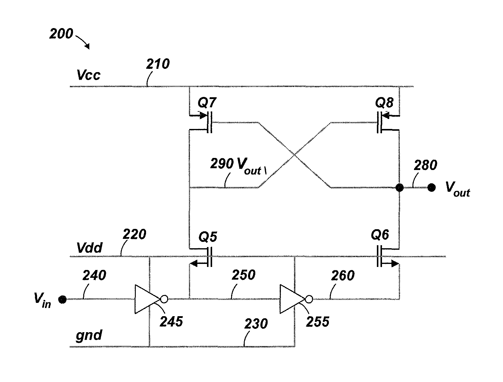
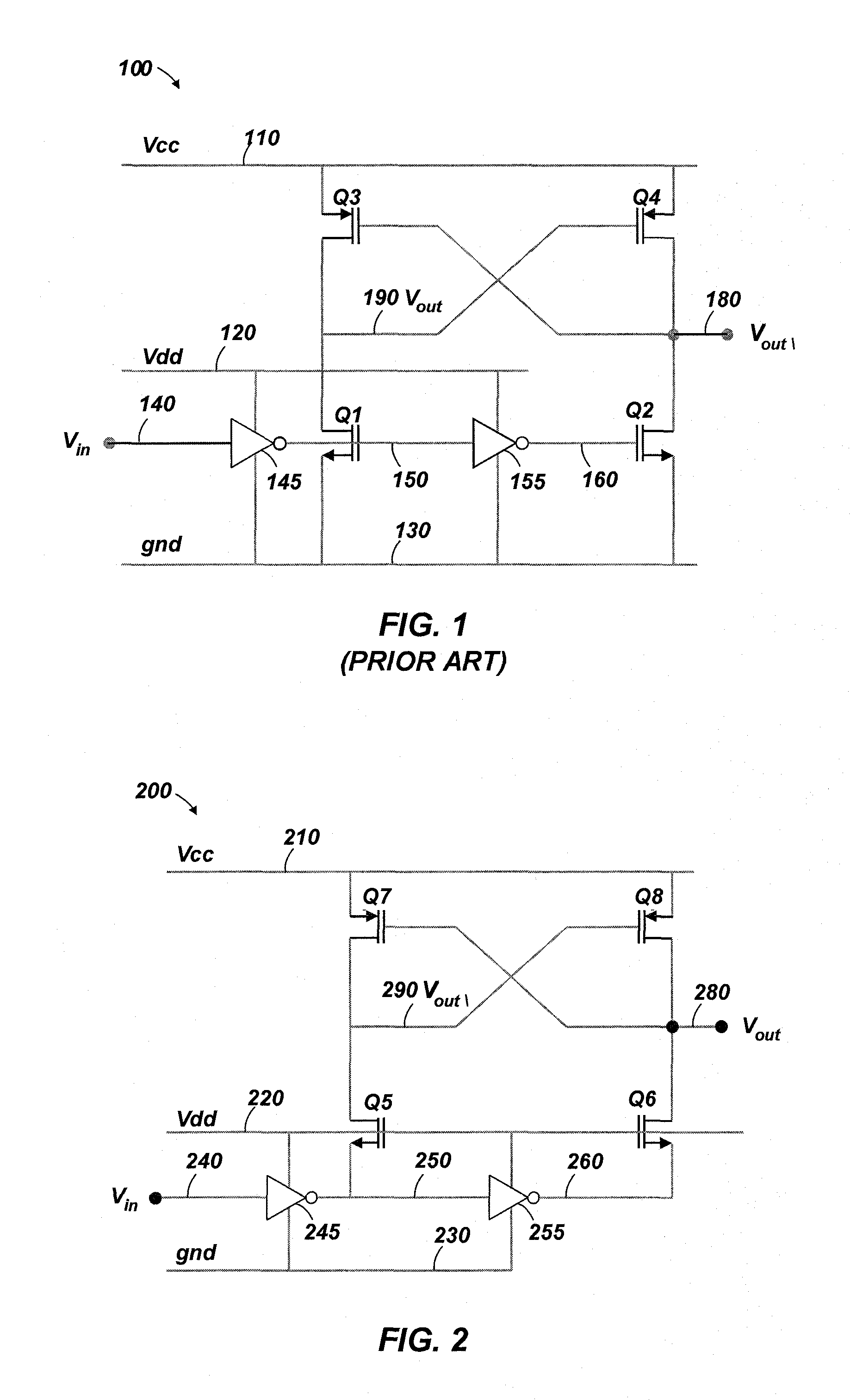
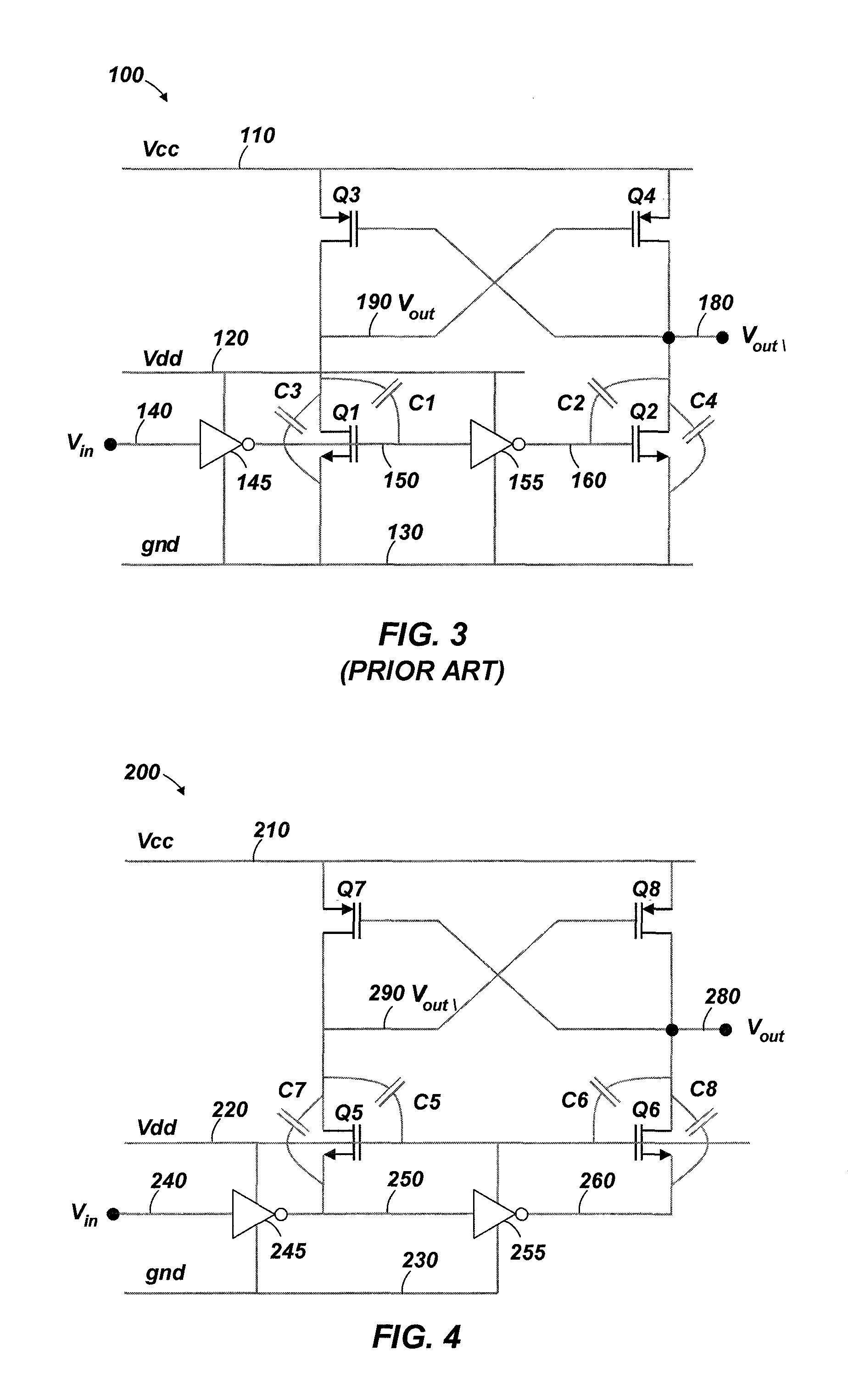
[0022]In the following description, elements, circuits, and functions may be shown in block diagram form in order not to obscure the present invention in unnecessary detail. Conversely, specific implementations shown and described are exemplary only and should not be construed as the only way to implement the present invention unless specified otherwise herein. Additionally, block definitions and partitioning of logic between various blocks is exemplary of a specific implementation. It will be readily apparent to one of ordinary skill in the art that the present invention may be practiced by numerous other partitioning solutions. For the most part, details concerning timing considerations and the like have been omitted where such details are not necessary to obtain a complete understanding of the present invention and are within the abilities of persons of ordinary skill in the relevant art.

[0023]Furthermore, in this description of embodiments of the invention, reference is made to ...


PUM


Abstract

Level shifting circuits and related methods are disclosed herein. The level shifting circuit includes a cross-coupled pull-up circuit coupled to a higher supply voltage, an output signal, and an inverted output signal. An input signal transitions between a ground and a lower supply voltage and an inverted input signal transitions in a direction opposite from the input signal between the ground and the lower supply voltage. A first n-channel transistor has a gate coupled to the lower supply voltage, a drain coupled to the output signal, and a source coupled to the inverted input signal. A second n-channel transistor has a gate coupled to the lower supply voltage, a drain coupled to the inverted output signal, and a source coupled to the input signal. The level shifting circuit may be included in an IC with core logic in a first voltage domain and input / output logic in a second voltage domain.

Description

TECHNICAL FIELD[0001]Embodiments of the present disclosure relate generally to voltage level shifting and, more particularly, to apparatuses and methods related to high voltage shifters that may have reduced output delays.BACKGROUND[0002]Advanced digital Integrated Circuit (IC) devices often have a low voltage logic core and relatively higher voltage Input / Output (IO) logic for interface with external components on a printed circuit board. As a result, voltage level translation circuits to translate from the low voltage domain to a high voltage domain are common and many such devices may be needed on an IC. Therefore, a logic level shifter that consumes minimum power and minimum die area while introducing minimum delay in the digital signal path is valuable to a very wide range of digital circuit applications including LCD panels, cell phones, MP3 players, microprocessors, memories, and many more devices.[0003]Level shift circuits (also referred to herein as level shifters) change t...

Claims


Application Information

Patent Timeline
Patent Type & Authority Patents(United States)
IPC IPC(8): H03K19/0175H03L5/00
CPCH03K3/35613
Inventor BARROW, JEFFREY G.
Owner INTEGRATED DEVICE TECH INC
Why Eureka
Try Eureka