Semiconductor optical amplifier

Inactive Publication Date: 2000-11-14
NEC CORP
View PDF14 Cites 21 Cited by
  • Summary
  • Abstract
  • Description
  • Claims
  • Application Information

AI Technical Summary

Problems solved by technology

However, it is not easy to fabricate accurately such an extremely narrow waveguid

Method used


Image

  • Semiconductor optical amplifier
  • Semiconductor optical amplifier
  • Semiconductor optical amplifier

Examples


Embodiment Construction

Referring to the drawings, the embodiment of the present invention is explained in detail.

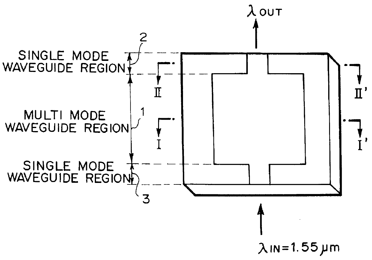
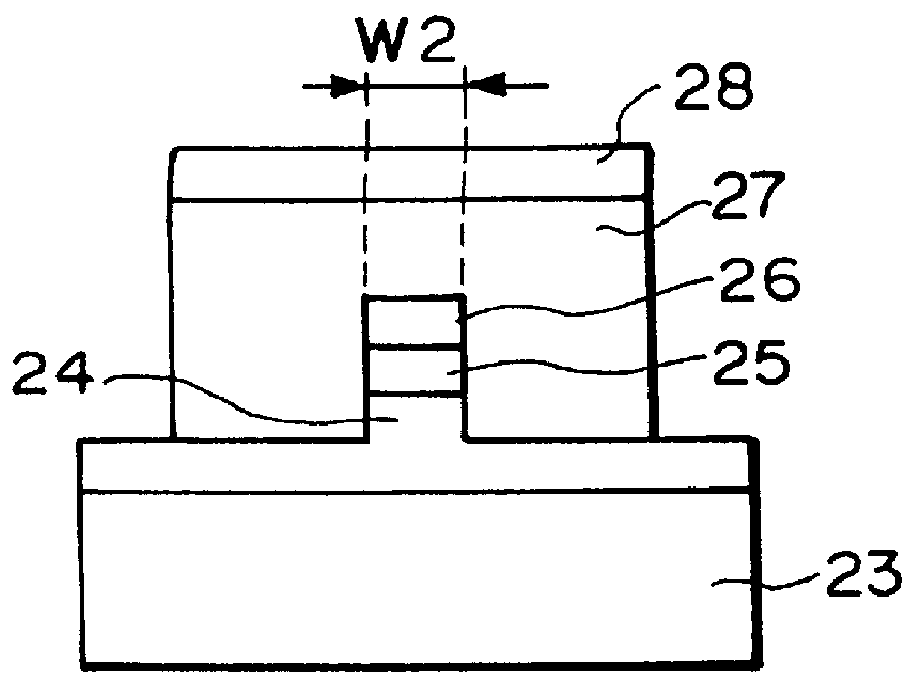
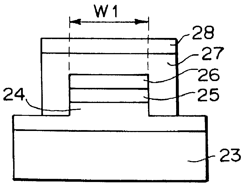
FIG. 1 is a perspective illustration of a 1.55 .mu.m band semiconductor optical amplifier of the present invention. The semiconductor optical amplifier comprises multi mode waveguide region 1, and single mode waveguide regions 2 and 3 each of which is connected with each end of the multi mode region 1. The length of the multi mode waveguide region 1 is about 340 .mu.m and the length of the single mode waveguide regions 2 and 3 is about 20 .mu.m. Accordingly, the length of the whole device is about 380 .mu.m. Multi mode waveguide region 1 is designed as a 1.times.1 multi mode interference (MMI) light waveguide. FIG. 2A is a cross sectional view taken on line I-I' to show the layered structure of the multi mode waveguide region, and FIG. 2B is a cross sectional view taken on line II-II' to show the layer structure of the single mode waveguide region. Both layer structures are the same except the ...


PUM


Abstract

A semiconductor optical amplifier wherein poalization independent gain, high saturation input light intensity, and high saturation gain are obtained. The semiconductor optical amplifier of the present invention comprises a 1x1 multi mode interference (MMI) light waveguide region and a couple of single mode waveguide regions, each of which is connected with each end of the multi mode region. The length of the multi mode waveguide region is about 340 mu m and the length of the single mode waveguide regions is about 20 mu m. The width of the multi mode waveguide region is about 12 mu m while the widths of the single mode waveguide regions 2,3 are about 1 mu m.

Description

1. Field of the InventionThe present invention relates to a polarization independent semiconductor optical amplifier with high saturation input and high saturation gain.2. Prior ArtRecently, the optical communication technology has been progressing as one of the technologies for a large capacity and high speed transmission. Amongst various optical communication technologies, a switching function of the semiconductor optical amplifiers as well as an amplifier function is of great interest, because the optical amplifier absorbs light without injection current.Preferably, the optical amplifier is expected to amplify signal light which passes through an optical fiber without controlling the polarization. Accordingly, the polarization independent gain is desirable.Therefore, various methods for implementing the polarization independent gain have been proposed. An example of the polarization independent semiconductor optical amplifier is reported in IEEE PHOTONICS TECHNOLOGY LETTERS(VOL.6...

Claims


Application Information

Patent Timeline
IPC IPC(8): G02B6/28H01S5/50H01S5/00H01S5/10G02B6/122H01S3/10
CPCG02B6/2813H01S5/5009H01S5/50H01S5/0655H01S5/1064
Inventor HAMAMOTO, KIICHI
Owner NEC CORP
Why Eureka
Try Eureka