Integrated circuit having reduced probability of wire-bond failure

a technology of integrated circuits and wire bonds, which is applied in the direction of semiconductor devices, semiconductor/solid-state device details, electrical apparatus, etc., can solve the problems of incomplete integrated circuit devices, extremely fragile flexible wire-bonds, and thin flexible wire-bonds,

Inactive Publication Date: 2000-11-28
BELL SEMICON LLC +1
View PDF1 Cites 6 Cited by
  • Summary
  • Abstract
  • Description
  • Claims
  • Application Information

AI Technical Summary

Problems solved by technology

Wire-bond failure at the pin level in integrated circuits is an important concern.
The wire-bonding between the various pads on the integrated circuit wafer chip and the pins is a delicate process, either performed by hand for small-volume productions, or performed by machine to fulfill high-volume needs.
Unfortunately, flexible wire-bonds are extremely fragile.
Moreover, the flexible wire bonds are very thin and thus are easily broken.
If any one wire-bond 552 fails (e.g., breaks or shorts to another wire-bond 552), it is likely that the entire integrated ...

Method used


Image

  • Integrated circuit having reduced probability of wire-bond failure
  • Integrated circuit having reduced probability of wire-bond failure
  • Integrated circuit having reduced probability of wire-bond failure

Examples


Embodiment Construction

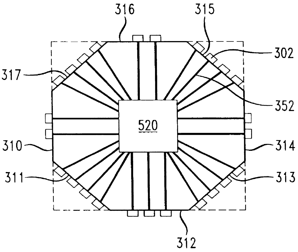
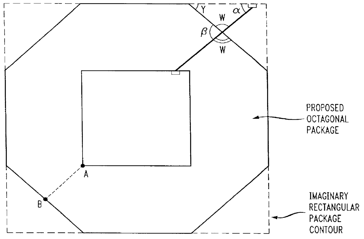
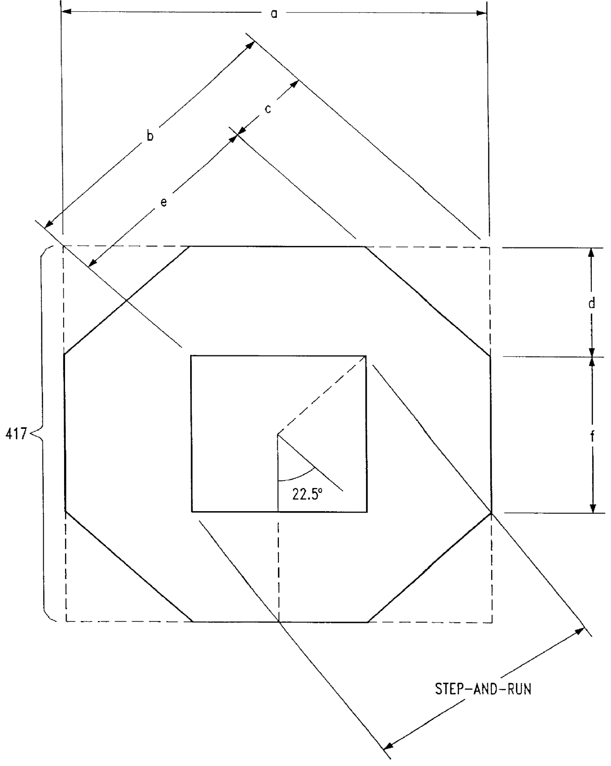
The present invention provides an improved integrated circuit having increasing reliability of wire-bond. In the integrated circuit, the contact angle between pins and their wire-bonds is increased in regions otherwise prone to wire-bond failure, i.e., in the corners of otherwise conventional integrated circuits.

In particular, a polygonal integrated circuit shape having at least five (5) pin supporting edges is introduced which provides a more optimum contact angle with respect to pins and their wire-bonds. While the disclosed embodiment relates particularly to an octagon-shaped integrated circuit package with a rectangular integrated circuit wafer chip, the principles of the present invention relate generally to any polygonal-shaped wire-bonding performed between pads on a rectangular integrated circuit chip wafer and at least five edges of a non-rectangular integrated circuit.

FIG. 1 shows an integrated circuit 300 including a square integrated circuit wafer chip (i.e., a die) 520,...


PUM


Abstract

The present invention provides an improved integrated circuit technique for increasing the reliability of wire-bonds in an integrated circuit by increasing the contact angle between certain pins and their respective wire-bonds, particularly those pins otherwise most susceptible to wire-bond failure, i.e., those pins conventionally located toward the corners of a conventional integrated circuit. By doing so, the overall length of the wire-bonds in a chip will be reduced, which in turn can result in further reduction of the probability of wire-bond failures. In a disclosed embodiment, a five or more sided integrated circuit shape is introduced wherein pads on up to four sides of an integrated circuit wafer chip are bonded to pins supported on eight edges of an integrated circuit package. An integrated circuit having at least five pin-supporting edges renders more robust wire-bond angles for any given integrated circuit package size.

Description

1. Field of the InventionThis invention relates generally to integrated circuits. More particularly, it relates to the design of a package shape improving the reliability of wire-bonds between an integrated circuit wafer chip and the input / output (I / O) pins of a packaged integrated circuit.2. Background of Related ArtWire-bond failure at the pin level in integrated circuits is an important concern. An integrated circuit can be rendered non-functional with even a single wire-bond failure.Integrated circuit wafer chips (i.e., "dies") are very small devices, often comprising tens or hundreds of thousands of transistors and other devices within an area much smaller than a dime. While many of the circuit connections are internal within an integrated circuit, it is also necessary to connect some of the internal wires with signals from external sources / sinks, e.g., with signals to and / or from other integrated circuits, with a power source, etc. Typically, electrical pads are formed on the ...

Claims


Application Information

Patent Timeline
IPC IPC(8): H01L23/48H01L23/498H01L23/12H01L23/13
CPCH01L23/13H01L23/49805H01L23/49811H01L2924/15162H01L2924/0002H01L2924/00
Inventor KERMANI, BAHRAM GHAFFARZADEH
Owner BELL SEMICON LLC
Why Eureka
Try Eureka