Digital CMOS-input with N-channel extended drain transistor for high-voltage protection

a digital cmos and high-voltage protection technology, applied in the field of electronic circuits, can solve the problems of high cost, high cost, and high cost of semiconductor fabrication, and achieve the effect of low cos

Active Publication Date: 2007-06-26
DIALOG SEMICONDUCTOR GMBH
View PDF8 Cites 27 Cited by
  • Summary
  • Abstract
  • Description
  • Claims
  • Application Information

AI Technical Summary

Benefits of technology

[0013]A principal object of the present invention is to realize a circuit for implementing an input port with an intrinsic high-voltage protection feature in form of very manufacturable integrated circuits at low cost.
[0014]Another principal object of the present invention is to provide an effective and very manufacturable method to implement circuits for signal processing, control operations, automation and computing and the like comprising low-voltage and high-voltage circuit blocks and incorporating input port devices for digital and / or analog input signals.
[0017]Further another object of the present invention is to give a method featuring the design of a high-voltage input port protection for low-voltage circuits, whereby the low-voltage parts are operating only with low-voltage signals.
[0018]Another further object of the present invention is to reduce the cost of manufacturing by implementing the circuit as a monolithic integrated circuit in low cost CMOS technology.
[0019]Also an object of the present invention is to reach a low-cost realization with modern integrated circuit technologies where a combined usage of high and low voltages on a port / circuit is realized using only CMOS devices.
[0020]Another still further object of the present invention is to reduce cost by using only CMOS devices, therefore making use of very economic chip design and production only in one technology with no additional process steps or devices other than CMOS.

Problems solved by technology

Therefore, when higher voltage operations take place sometimes DMOS (Double Diffused MOS) transistor devices are used, making necessary an expensive process in semiconductor fabrication.
Alternatively CMOS devices with extended drain realizations are employed, but when used in a differential input pair transistor configuration, high VGS (Gate-Source) values for the transistors have to be specified, which leads also to more expensive components.
Thereto an appropriately combined semiconductor technology capable of handling all these demands is chosen, which also most often leads to costly solutions.
The challenge for the designer of such circuits is therefore to find a reliable, efficient and cost effective solution.
These technologies are expensive however and it is desirable to find solutions that are less expensive.
However these approaches use often solutions, which are somewhat technically complex and therefore also expensive in production.
Preferred prior art realizations are implementing protection means differently, more complex in function and more expensive in production.
It is therefore a challenge for the designer of such circuits to achieve a high-quality, but lower-cost solution.
The circuit design topology also limits the number of devices that are exposed to high voltage.

Method used


Image

  • Digital CMOS-input with N-channel extended drain transistor for high-voltage protection
  • Digital CMOS-input with N-channel extended drain transistor for high-voltage protection
  • Digital CMOS-input with N-channel extended drain transistor for high-voltage protection

Examples


Embodiment Construction

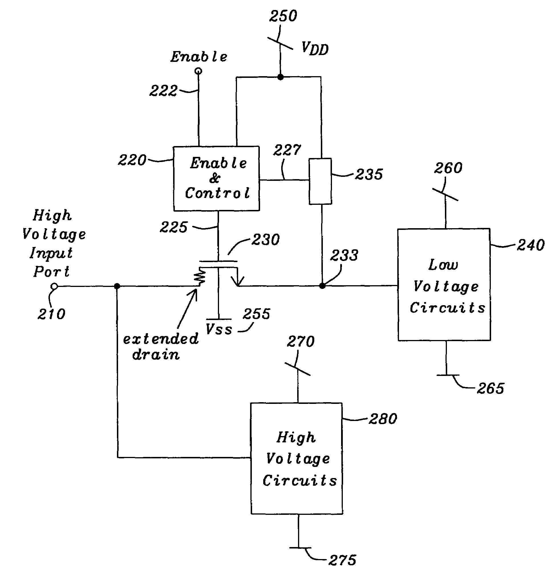
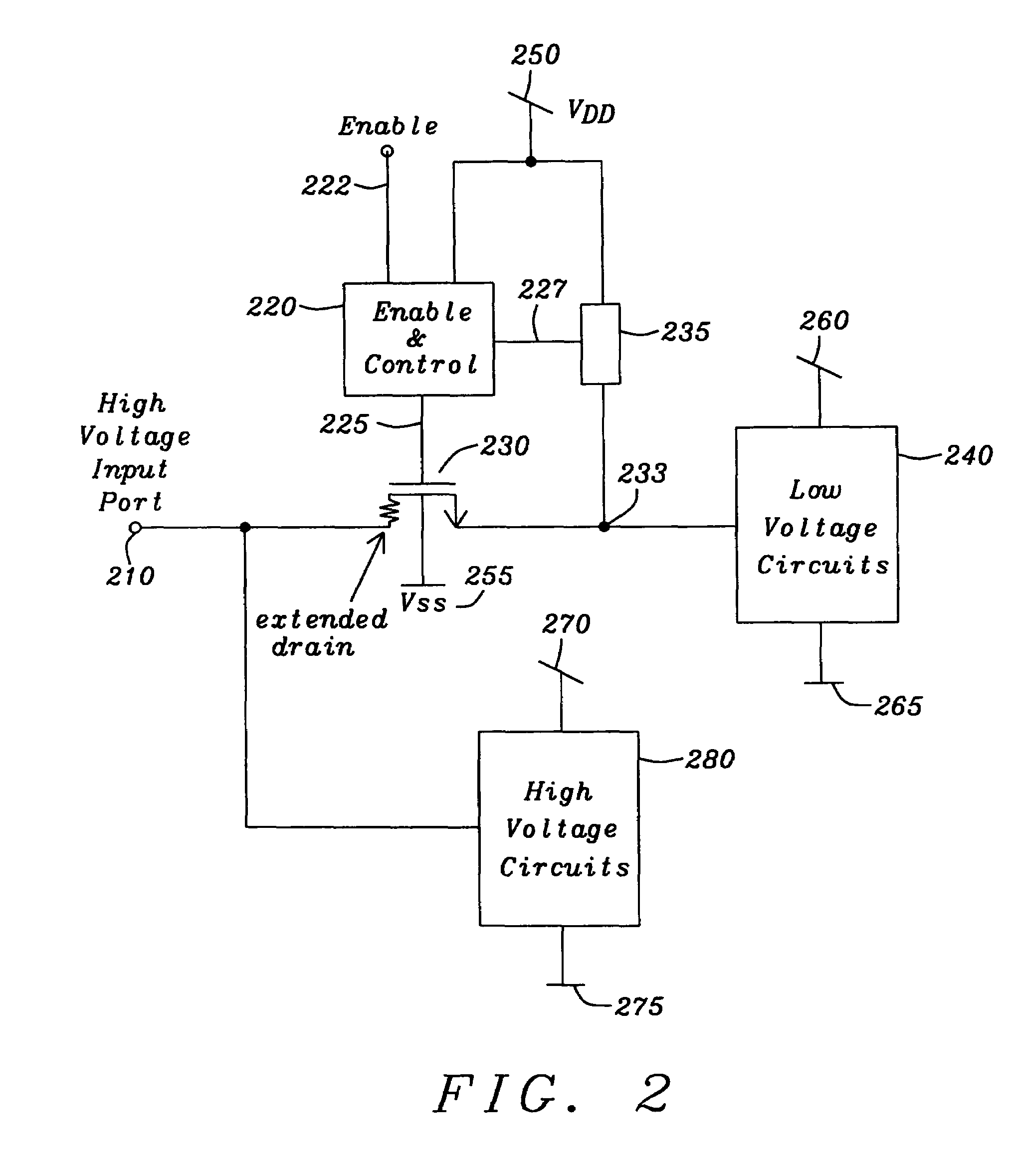
[0028]The preferred embodiment of the invention discloses a novel circuit for an input port device, which can be used as interface between a high voltage circuit—or a low voltage circuit of course—by protecting the access to internal low voltage CMOS circuit parts of said input port bearing circuit with the help of a low voltage CMOS n-channel transistor with extended drain. In contrast to current practice where low voltage circuits or ports can only be used in the low voltage domain and not together with high voltage applications this solution avoids the disadvantages of providing extra ports or circuits or additional process steps for special protection devices e.g. in DMOS technology in order to enable such high voltage applications.

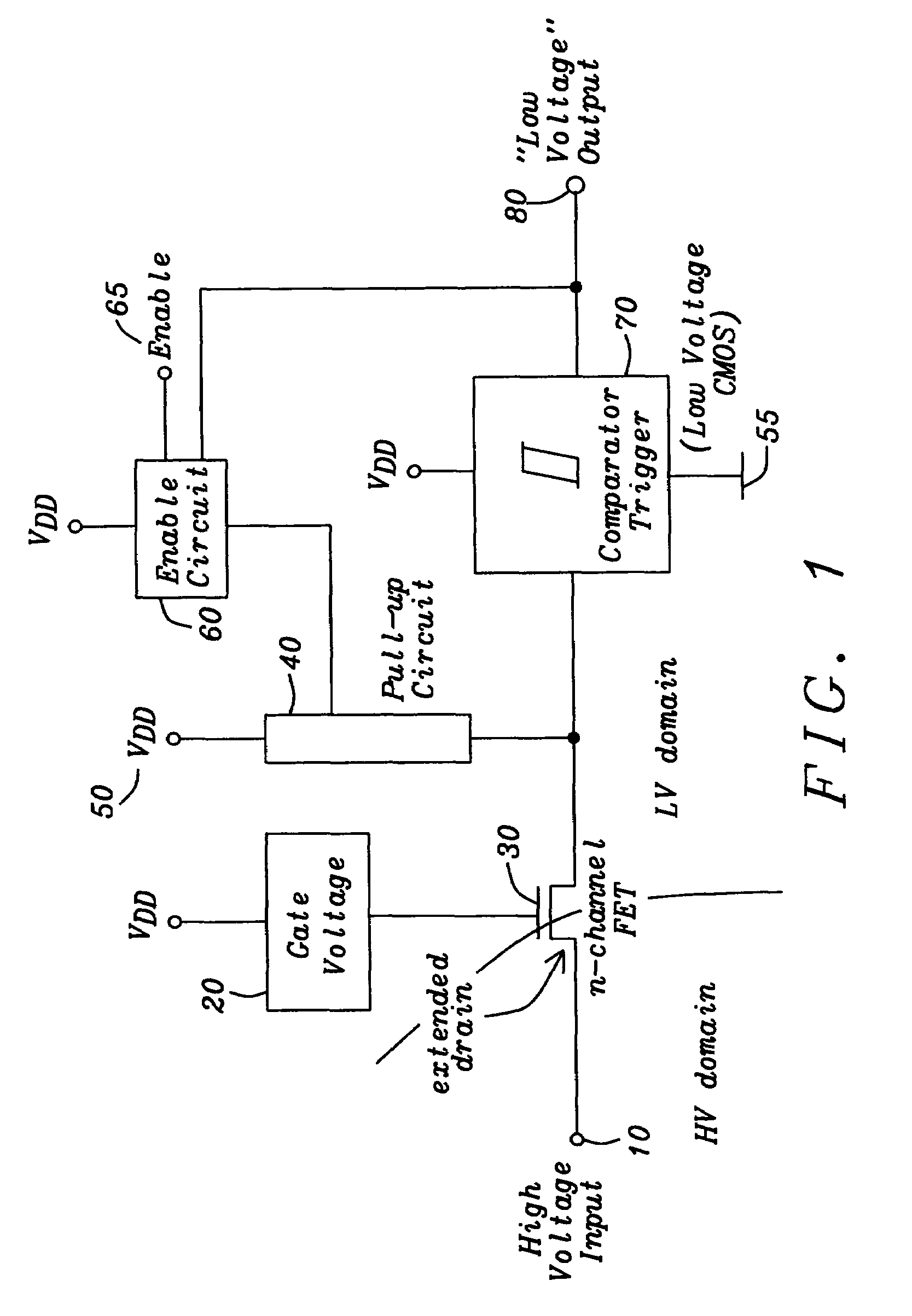
[0029]Looking now at FIG. 1 showing a schematic diagram of the basic circuit of an input port device according to the invention a High Voltage (HV) Input terminal 10 is observed, connected to the drain (implemented in extended drain technology) of a s...


PUM


Abstract

A circuit and a method are given, to realize an electronic system for combined usage at differing voltage ranges as defined by a low-voltage range for operating standard CMOS devices and a high-voltage range exceeding said standard CMOS low-voltage operating range significantly by multiples and thus necessarily utilizing input ports with an intrinsic high-voltage protection feature. Said circuit and method are designed in order to be implemented with a very economic number of components, capable to be realized with standard modern integrated circuit technologies in CMOS technology.

Description

BACKGROUND OF THE INVENTION[0001]1. Field of the Invention[0002]The present invention relates generally to electronic circuits for higher voltages and in particular to protect low voltage circuits realized with integrated-circuit technologies. Somewhat more in particular the current invention is also relating to switch controller circuits and more particularly, to integrated circuits for motor bridge interfaces, and even more particularly to circuits controlling MOS power transistors within an H-bridge configuration for DC-motor driving applications.[0003]2. Description of the Prior Art[0004]In many technical fields, where automation is of the utmost importance in order to reach a comfortable and reliable operation for users, like production of modern vehicles, manufacture of electrical and electronical household appliances, data processing or computing devices and telecommunications equipment, or industrial use of precision tooling machines etc. nowadays mixed signal integrated cir...

Claims


Application Information

Patent Timeline
Patent Type & Authority Patents(United States)
IPC IPC(8): H03K19/007
CPCH03K19/00315H03K19/018507
Inventor SALZMANN, OLIVERKRENZKE, RAINER
Owner DIALOG SEMICONDUCTOR GMBH
Why Eureka
Try Eureka