Substrate for reducing electromagnetic interference and enclosure

a technology of electromagnetic interference and substrate, applied in the field of substrate, can solve the problems of interference or degradation of signals traveling along other traces, malfunctions of nearby electrical devices, and more emi problems

Inactive Publication Date: 2001-02-20
INTEL CORP
View PDF29 Cites 118 Cited by
  • Summary
  • Abstract
  • Description
  • Claims
  • Application Information

AI Technical Summary

Problems solved by technology

Electromagnetic interference ("EMI") can cause several problems, such as malfunctions of nearby electrical devices and interference or degradation of signals traveling along other traces.
EMI problems have resulted in the Federal Communications Commission adopting guidelines

Method used


Image

  • Substrate for reducing electromagnetic interference and enclosure
  • Substrate for reducing electromagnetic interference and enclosure
  • Substrate for reducing electromagnetic interference and enclosure

Examples


Embodiment Construction

Illustrative embodiments of the invention are described below. In the interest of clarity, not all features of an actual implementation are described in this specification. It will of course be appreciated that in the development of any such actual embodiment, numerous implementation-specific decisions must be made to achieve the developers' specific goals, such as compliance with system-related and business-related constraints, which will vary from one implementation to another. Moreover, it will be appreciated that such a development effort might be complex and time-consuming, but would nevertheless be a routine undertaking for those of ordinary skill in the art having the benefit of this disclosure.

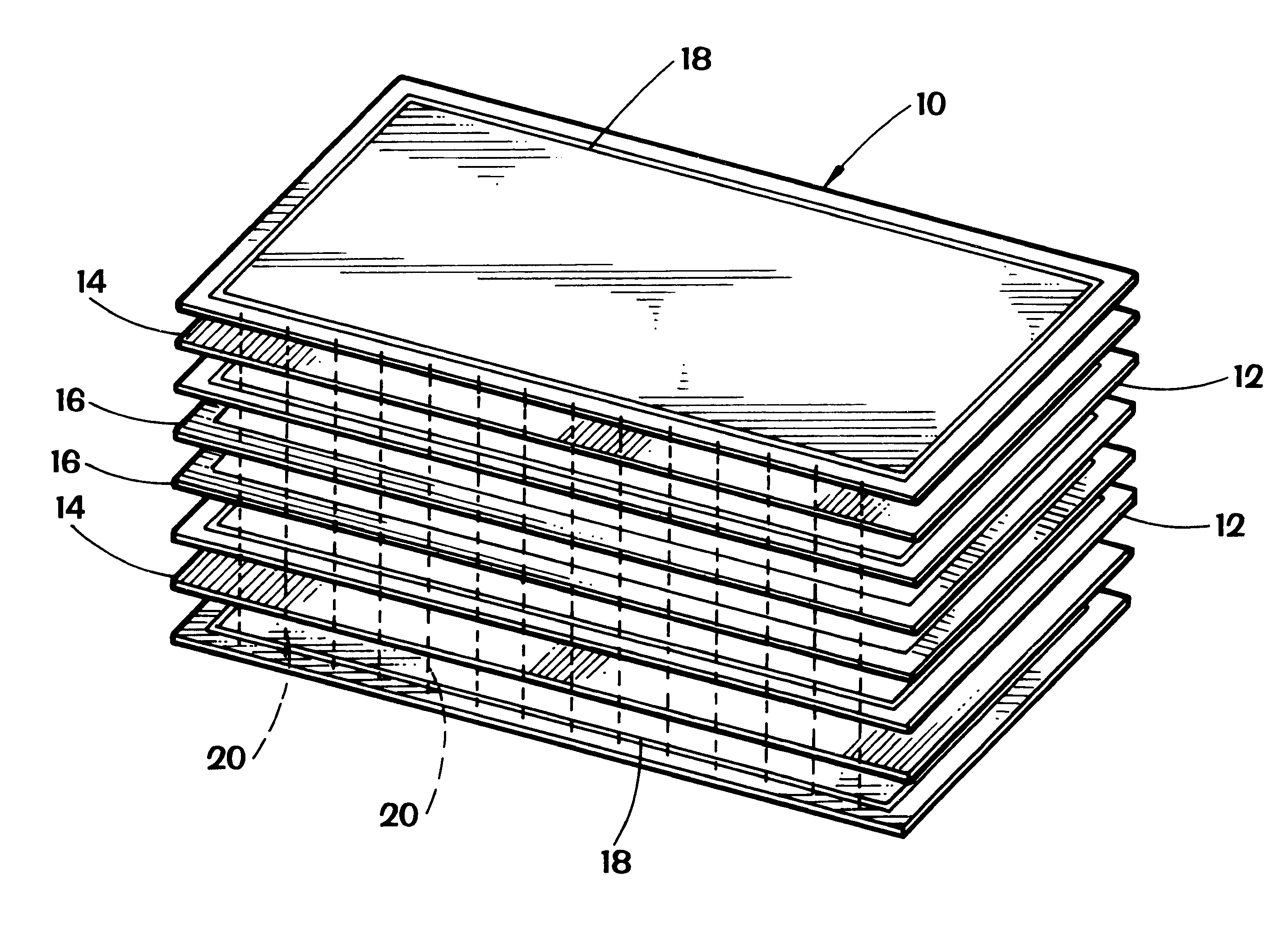
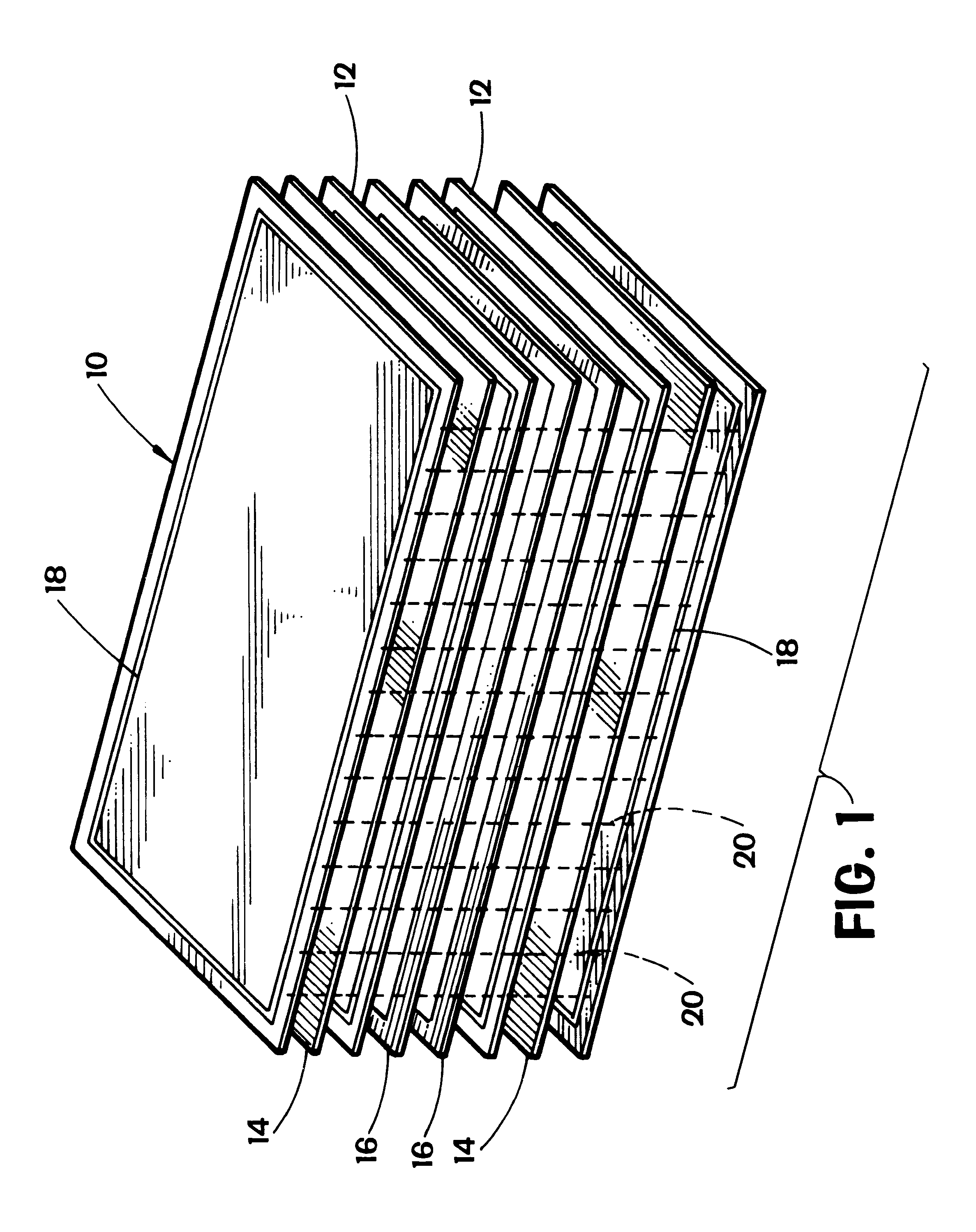
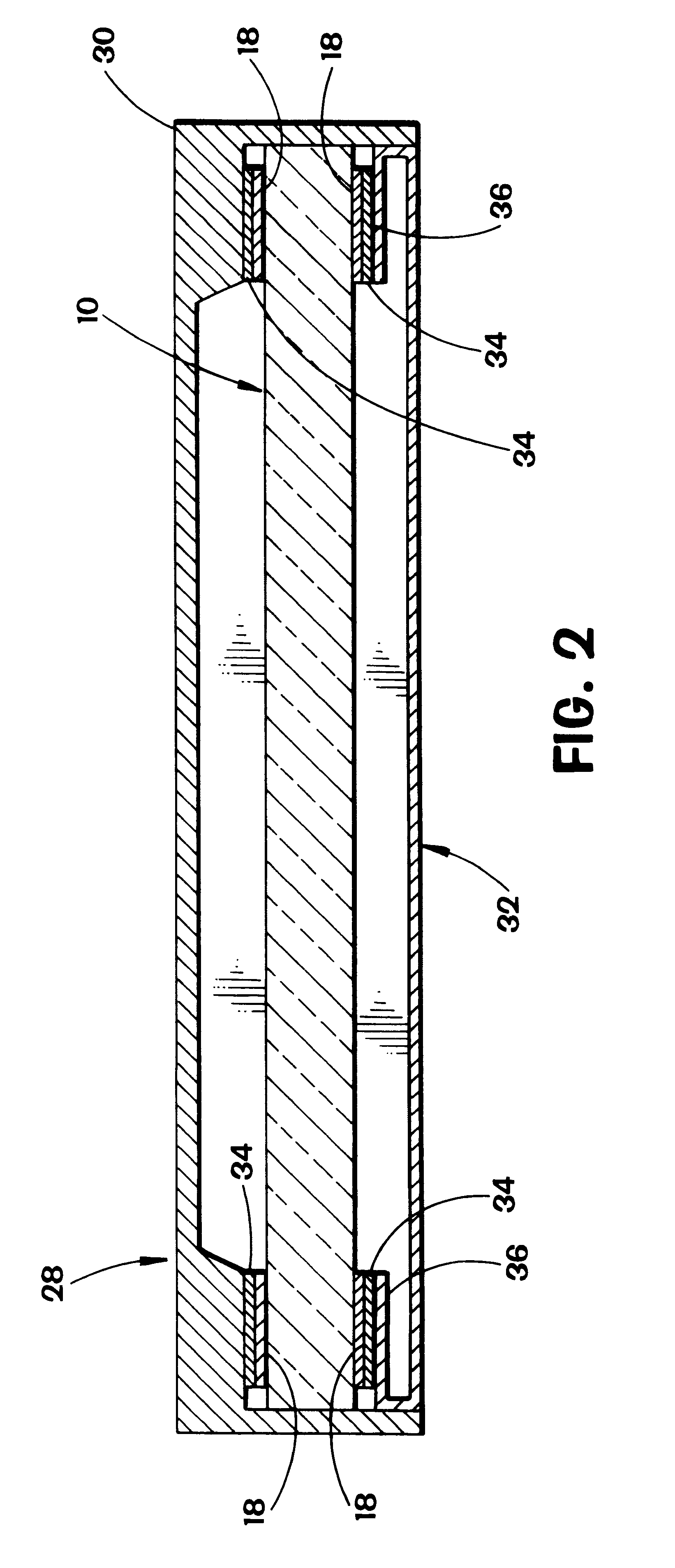
Turning now to the drawings, and particularly to FIG. 1, a perspective, exploded view of a substrate 10 for mounting various integrated circuit components is shown. The substrate 10 may be comprised of multiple signal layers 12, ground layers 14, and power layers 16. Ground rings 18 ma...


PUM


Abstract

A substrate for reducing electromagnetic emissions is provided. The substrate may include a plurality of ground layers, signal layers and power layers. All of the layers other than the ground layer are provided with a ground ring that may extend around the perimeter of the layer. The ground rings are electrically coupled together by ground stitching or vias that are randomly spaced. The random spacing of the ground stitching is based on the operating frequencies of the integrated circuit devices mounted on the substrate. Additional shielding may be provided by providing a cover assembly made of any conductive material that is coupled to the exposed ground rings on the uppermost and lowermost surfaces of the substrate. The cover assembly is coupled to the exposed ground rings in a randomized pattern. The device provides a virtual electrical ground cage in which the internal signal layers are totally enclosed, thereby reducing electromagnetic emissions.

Description

1. Field of the InventionThis invention relates generally to a substrate upon which integrated circuit components are mounted and, more particularly, to a substrate that reduces electromagnetic emissions and associated electromagnetic interference problems.2. Description of the Related ArtIn the field of electronics, various integrated circuit components, such as microprocessors, are commonly mounted on a substrate. This substrate is typically comprised of ground layers, signal layers, and power layers. The signal layer contains traces that allow the transmission of various signals between the various integrated circuit components positioned on the substrate.It is well known in the art that signals traveling within these traces can produce electromagnetic emissions, i.e., radiated electrical fields. Electromagnetic interference ("EMI") can cause several problems, such as malfunctions of nearby electrical devices and interference or degradation of signals traveling along other traces...

Claims


Application Information

Patent Timeline
IPC IPC(8): H01L23/552H05K9/00H05K1/02
CPCH01L23/552H05K1/0218H05K9/0039H01L2924/0002H01L2924/00
Inventor SKINNER, HARRY G.DELAPLANE, NEIL C.MAHAJAN, RAVI V.STARKSTON, ROBERTLII, MIRNG-JIEDSALL, RON
Owner INTEL CORP
Why Eureka
Try Eureka