Semiconductor device and method for producing the same

a semiconductor and field-effect technology, applied in semiconductor devices, digital storage, instruments, etc., can solve the problems of tft defects and substantial breakage of gate electrodes

Inactive Publication Date: 2001-03-13
SEMICON ENERGY LAB CO LTD
View PDF30 Cites 48 Cited by
  • Summary
  • Abstract
  • Description
  • Claims
  • Application Information

AI Technical Summary

Problems solved by technology

A problem of such TFT is that the presence of recessed portion 27 causes substantial break of the gate electr

Method used


Image

  • Semiconductor device and method for producing the same
  • Semiconductor device and method for producing the same
  • Semiconductor device and method for producing the same

Examples


Embodiment Construction

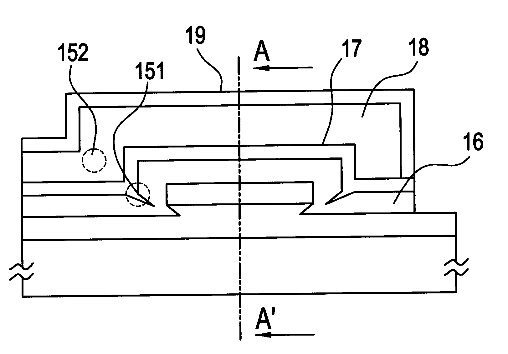
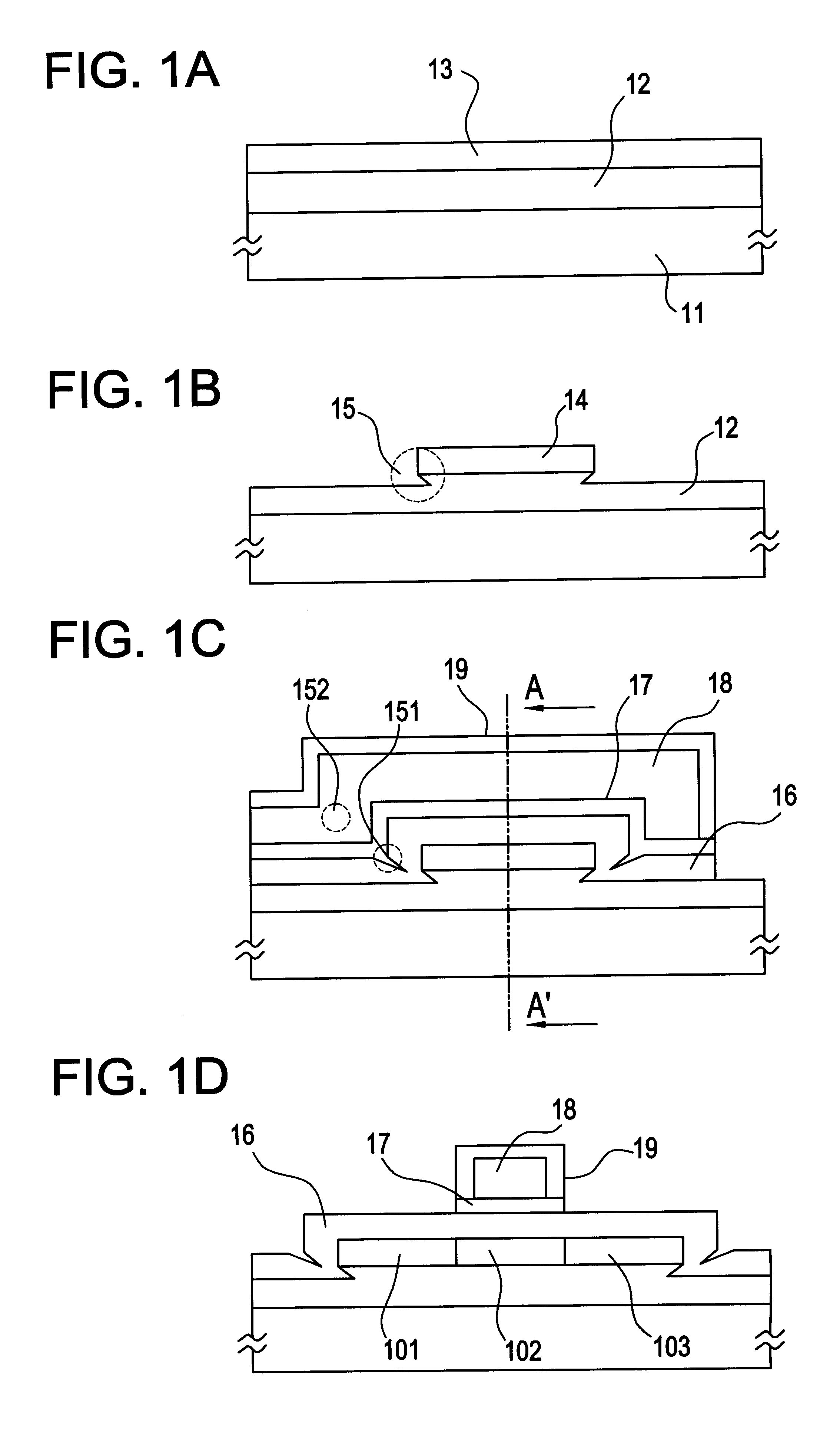
FIGS. 1A to 1D illustrate the procedure for producing an N-channel thin film transistor (TFT) of an embodiment of this invention. Although the embodiment describes the production procedure for an N-channel TFT, a P-channel TFT may be applied for this invention. The TFT of the embodiment is applicable for TFTs formed at a peripheral circuit or at a pixel area in a liquid crystal display unit, and further for TFTs in integrated circuits.

The silicon oxide film 12 as the base film is formed at a thickness of 2000 .ANG. on the glass substrate 11 using a sputtering method. The amorphous silicon film 13 is formed at a thickness of 1000 .ANG. by plasma CVD method. The formed silicon film 13 is crystallized by heating, irradiating laser beam, irradiating intense light, etc. A crystalline silicon film may be formed directly by vapor deposition method instead of the amorphous silicon film 13, and the amorphous film may be left non-crystallized. The element separation patterning is conducted to...


PUM


Abstract

In the production of thin film transistor (TFT), a gate insulating film is formed to cover an active layer, a titanium nitride film is formed on the gate insulating film, and an aluminum film used as the gate electrode is formed on the titanium nitride film. The resulted configuration prevents the etching of the aluminum film from the insulating film side even if the etchant of aluminum enters the recessed portion at the edge of the active layer during the patterning of the gate electrode. Also in the anodizing process, when an oxide film is formed on the surface of the aluminum film, the oxidation of aluminum from the gate insulating film side is prevented even when the electrolyte solution enters the recessed portion at the edge of the active layer.

Description

1. Field of the InventionThis invention relates to an insulated gate field effect semiconductor device using a thin film semiconductor and a method for producing the same.2. Description of the Related ArtA known structure of an insulated gate field effect transistor using a thin film semiconductor (hereinafter referred to simply as "TFT") is shown in FIG. 2D. The method for producing such TFT is described below with reference to FIGS. 2A to 2D.A base film (silicon oxide film) 22 is formed on a glass substrate 21 at a thickness of approximately 2000 .ANG.. On the base film 22, a silicon semiconductor layer 23 having amorphous or crystalline structure is formed as an active layer (where source / drain regions and a channel forming region are formed) at a thickness of about 1000 .ANG. to obtain the shape shown in FIG. 2A. An element separation patterning is performed to obtain a shape shown in FIG. 2B. During this patterning, it is difficult to etch only the active layer 23, and the base...

Claims


Application Information

Patent Timeline
IPC IPC(8): G11C11/56H01L21/02H01L21/336H01L29/49H01L29/423H01L29/40H01L21/28H01L29/78H01L29/786
CPCG11C11/56G11C11/5692H01L29/42384H01L29/4908H01L29/66757H01L29/78603H01L27/12
Inventor MIYAZAKI, MINORUMURAKAMI, AKANETERAMOTO, SATOSHI
Owner SEMICON ENERGY LAB CO LTD
Why Eureka
Try Eureka