

Overvoltage protection device
- Summary
- Abstract
- Description
- Claims
- Application Information
AI Technical Summary
Benefits of technology
Problems solved by technology
Method used
Image

Examples
first embodiment
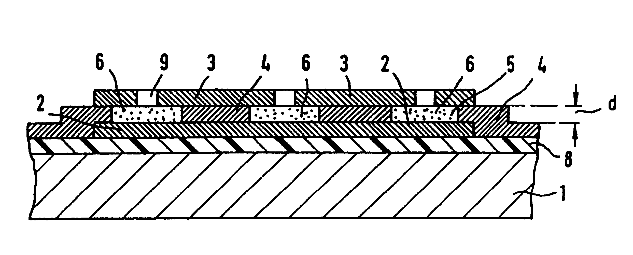
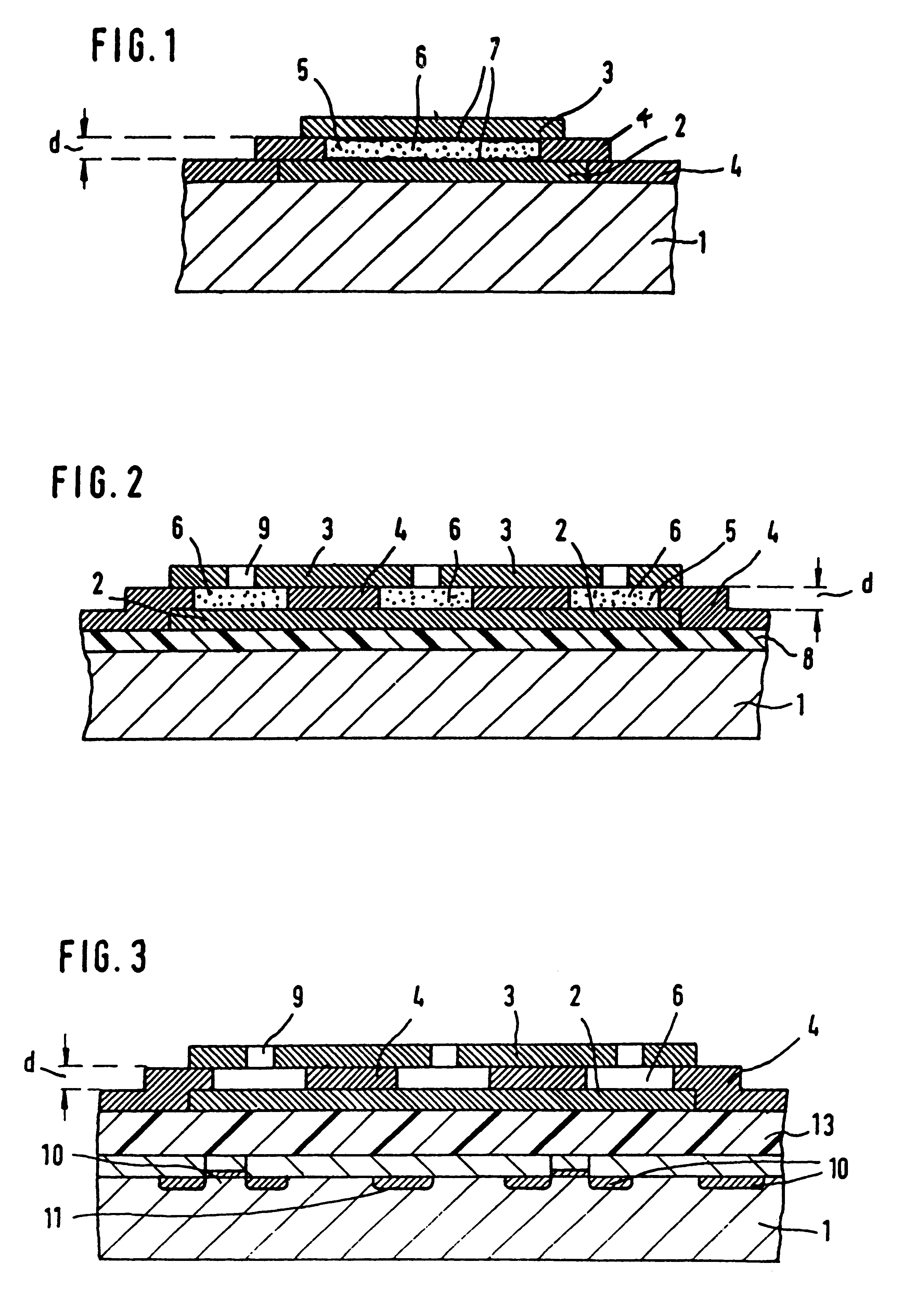
the process according to the invention will now be described with reference to FIG. 2. The substrate 1 is covered with the insulating layer 8. On the insulating layer 8, the first electrode layer 2 is formed, which is covered with the spacing layer 4. The spacing layer 4 is covered with the second electrode layer 3, in which windows 9 are formed. The different layer on the substrate 1 are formed by conventional microelectronic circuit fabrication processes. One example is semiconductor process technology, with the substrate 1 being a semiconductor substrate. The spacing layer 4 is formed from a material having a substantially greater etch rate than the material of the electrode layers 2, 3. The spacing layer 4 is etched through the window 9 from the surface of the second electrode layer 3. The different etch rates of the materials of the spacing layer 4 and the electrode layers 2, 3 cause an undercutting effect: The material of the first electrode layer 2 and that of the second elec...
second embodiment
In the process according to the invention, the insulating layer 8, the first electrode layer 2 and the spacing layer 4 are deposited in a manner analogous to that in the process just described. Next, the openings 5 are formed in the spacing layer 4. This is done by techniques commonly used in microelectronic circuit fabrication technology, particularly by conventional masking and etching techniques. After that, a sheetlike material is placed as the second electrode layer 3 on the spacing layer 4 and joined to the latter, either permanently, for example by bonding, or nonpermanently, for example by clamping. In the embodiment shown, the sheetlike material has windows 9 which register with the openings 5 of the spacing layer 4.
PUM
 Abstract
Description
Claims
Application Information