Area array stud bump flip chip device and assembly process
- Summary
- Abstract
- Description
- Claims
- Application Information
AI Technical Summary
Benefits of technology
Problems solved by technology
Method used
Image

Examples
Embodiment Construction
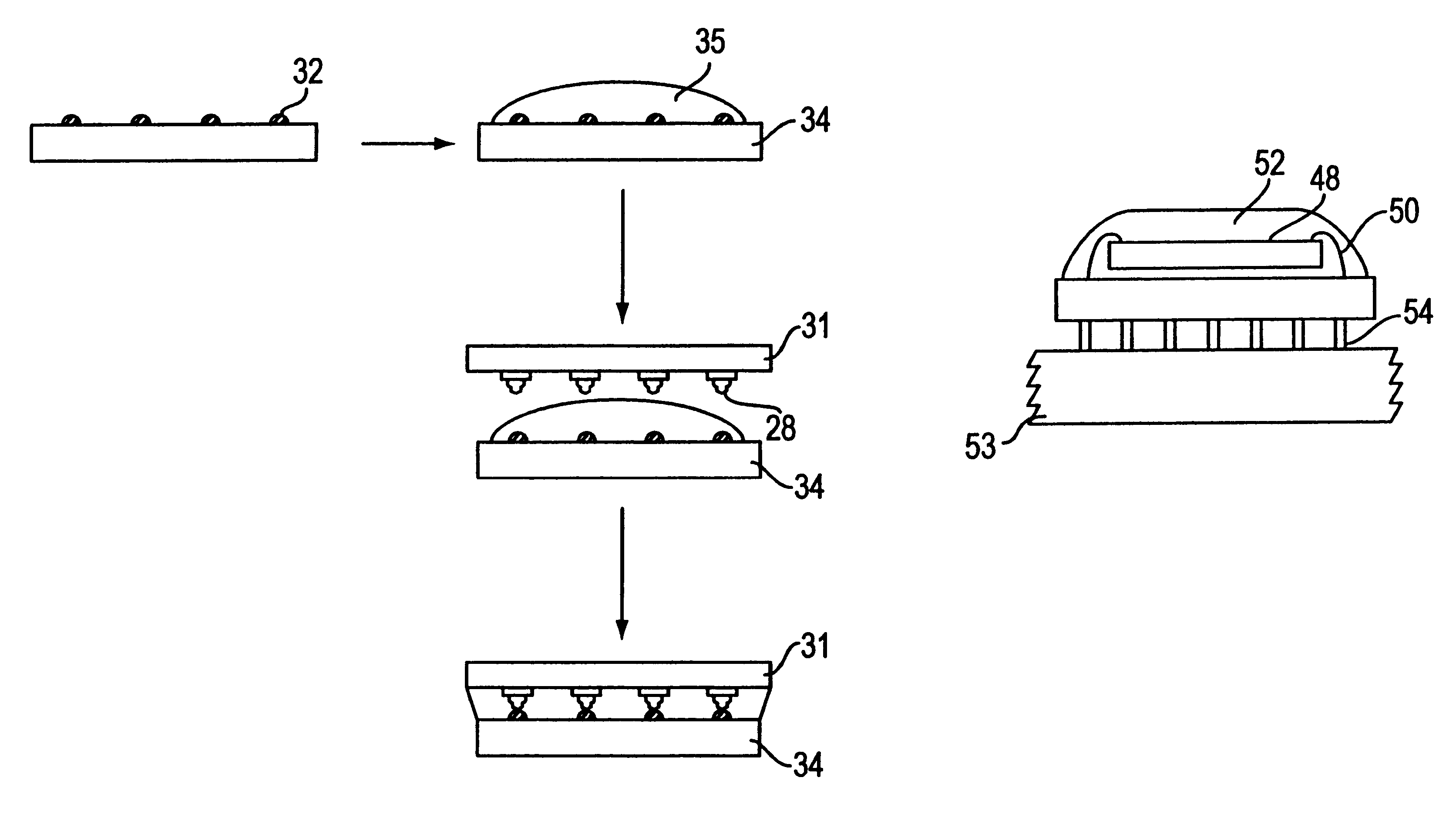
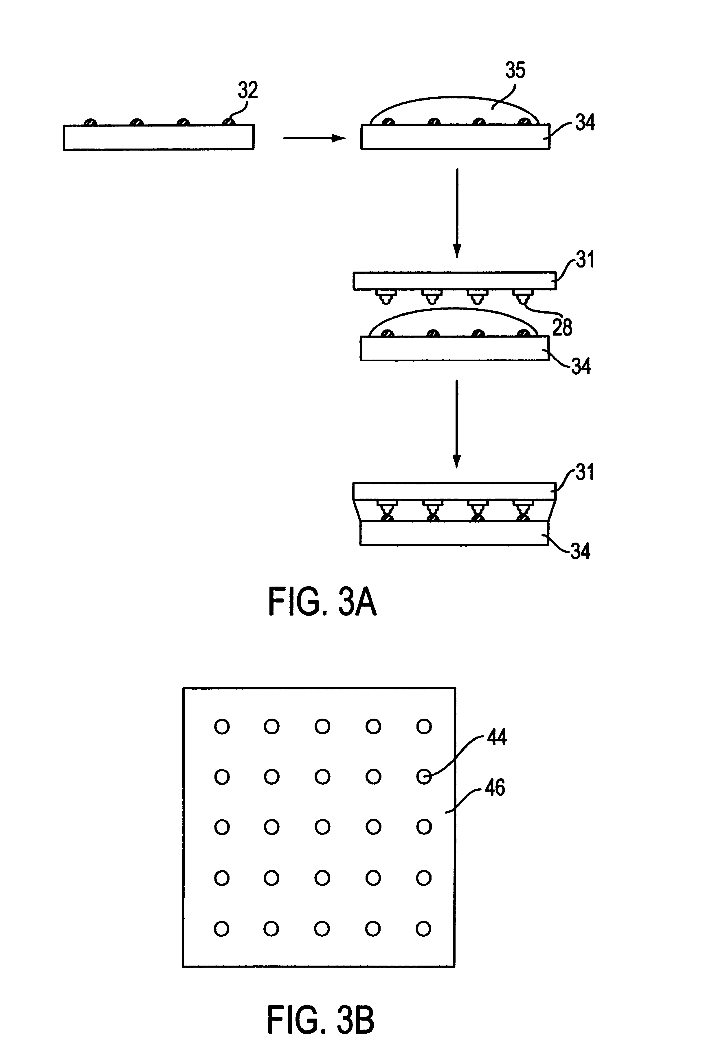
The present invention is a flip chip device produced by stud-bumping method. where the stud bumps are bonded to the substrate. This completely eliminates the limitation of not being able to have interconnections over the active area of the chip, and allows the stud bump interconnection method to be applied over the entire chip area to give an area array. This unexpected outcome allows wire bonding technology to be applied to area array flip chips, comparable to the flip chip solder joint interconnection method.
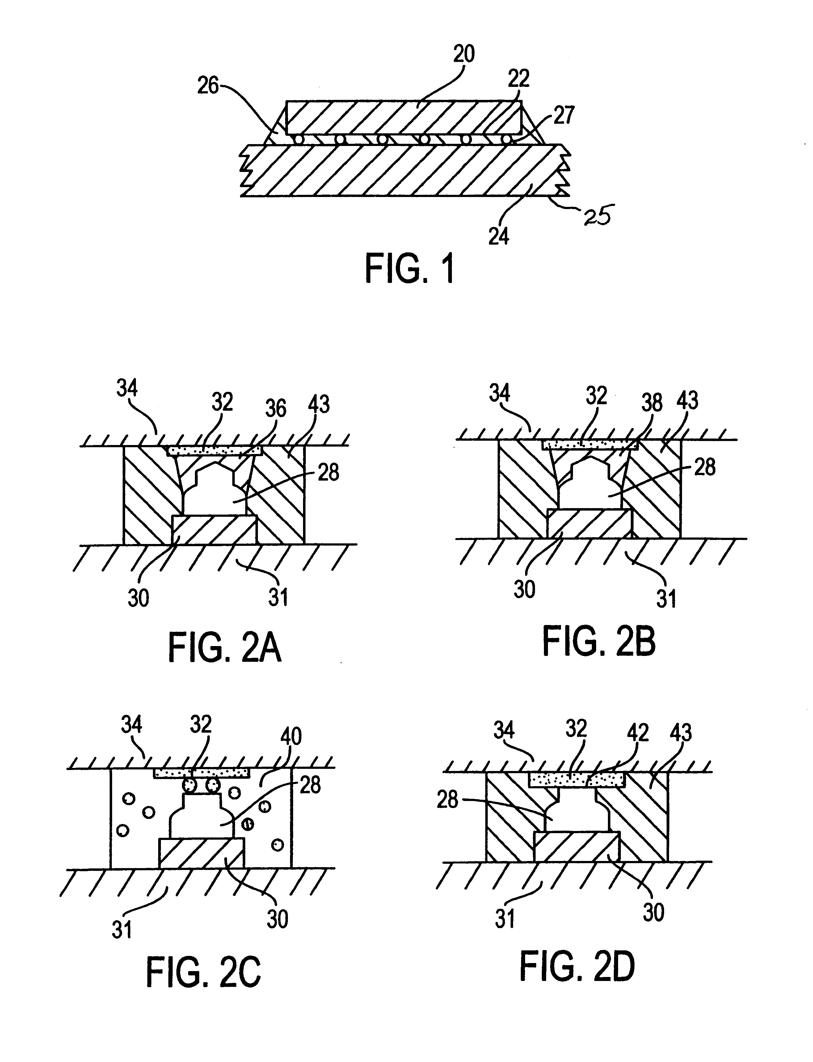
FIG. 1 shows a diagram of a generic flip chip on a first level electronic substrate, with a semiconductor chip 20 having the active surface 22 facing downwards towards the electronic substrate 24. Surface 25 is the exterior surface of the substrate which may also contain exterior I / O pads for interconnection with second level substrates. These first and second level substrates may be a single or multilayer organic substrate, a ceramic substrate, a printed circuit laminate in c...
PUM
 Abstract
Description
Claims
Application Information
 - Generate Ideas
- Intellectual Property
- Life Sciences
- Materials
- Tech Scout
- Unparalleled Data Quality
- Higher Quality Content
- 60% Fewer Hallucinations
Browse by: Latest US Patents, China's latest patents, Technical Efficacy Thesaurus, Application Domain, Technology Topic, Popular Technical Reports.
© 2025 PatSnap. All rights reserved.Legal|Privacy policy|Modern Slavery Act Transparency Statement|Sitemap|About US| Contact US: help@patsnap.com