Plastic package material through hole and filling method thereof

A technology of plastic packaging materials and filling methods, applied in the direction of electrical components, electrical solid devices, circuits, etc., to achieve the effect of avoiding too rough, good electrical interconnection effect, and simple steps

Active Publication Date: 2017-05-31
SJ SEMICON JIANGYIN CORP
View PDF5 Cites 0 Cited by
  • Summary
  • Abstract
  • Description
  • Claims
  • Application Information

AI Technical Summary

Problems solved by technology

In order to electrically connect components in different layers, via technology can be used to provide electrical interconnection and provide mechanical support, and there is currently no effective method for filling mold compound vias

Method used


Image

  • Plastic package material through hole and filling method thereof
  • Plastic package material through hole and filling method thereof
  • Plastic package material through hole and filling method thereof

Examples


Embodiment 1

[0061] This embodiment provides a method for filling via holes of plastic encapsulants, the filling method comprising:

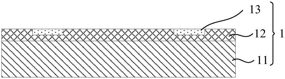
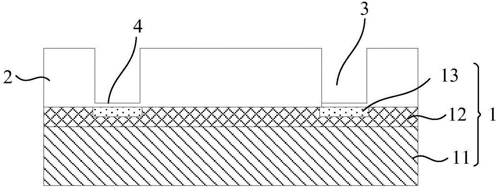
[0062] S1: providing a metal pad structure 1, and forming a plastic encapsulation material layer 2 on the upper surface of the metal pad structure 1;

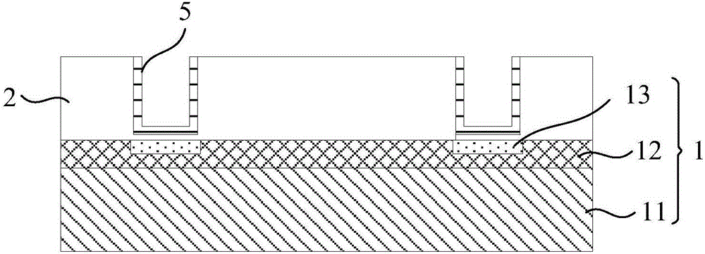
[0063] S2: Form an opening 3 on the molding material layer 2 corresponding to the position of the metal pad 13, and form a barrier layer 5 on the inner surface of the opening 3, wherein a predetermined thickness of the molding material layer remains above the metal pad 13 as protective layer 4;

[0064] S3: removing the barrier layer 5 and the protective layer 4 at the bottom of the opening 3, exposing the metal pad 13;

[0065] S4: Forming a seed layer 6 on the surface of the barrier layer 5 and the upper surface of the metal pad 13, and forming a metal layer 7 and a polymer layer 8 on the surface of the seed layer 6 in sequence.

[0066] see belowFigure 1 to Figure 4 The method for filling the via holes o...

Embodiment 2

[0096] This embodiment provides a method for filling via holes of plastic encapsulants, the filling method comprising:

[0097] S1: providing a metal pad structure 1, and forming a plastic encapsulation material layer 2 on the upper surface of the metal pad structure 1;

[0098] S2: Form an opening 3 on the molding material layer 2 corresponding to the position of the metal pad 13, and form a barrier layer 5 on the inner surface of the opening 3, wherein a predetermined thickness of the molding material layer remains above the metal pad 13 as protective layer 4;

[0099] S3: removing the barrier layer 5 and the protective layer 4 at the bottom of the opening 3, exposing the metal pad 13;

[0100] S4: Forming a seed layer 6 on the surface of the barrier layer 5 and the upper surface of the metal pad 13, and forming a metal layer 7 and a polymer layer 8 on the surface of the seed layer 6 in sequence.

[0101] see below Figure 5 to Figure 9 The method for filling the via hole...

Embodiment 3

[0137] Such as Figure 4 with Figure 9 As shown, this embodiment provides a via hole for molding compound, and the via hole for molding compound includes:

[0138] Metal pad structure 1;

[0139] A plastic encapsulant layer 2 located on the upper surface of the metal pad structure 1 and formed with a via hole at a position corresponding to the metal pad 13;

[0140] The barrier layer 5 located on the inner wall surface of the via hole;

[0141] a seed layer 6 located on the surface of the barrier layer 5 and the upper surface of the metal pad 13;

[0142] a metal layer 7 on the surface of the seed layer 6; and

[0143] A polymer layer 8 located on the surface of the metal layer 7 and filling the via hole.

[0144] As an example, the metal pad structure 1 includes:

[0145] carrier plate 11;

[0146] a redistribution layer 12 located on the upper surface of the carrier 11; and

[0147] At least one metal pad 13 located on the redistribution layer 12 .

[0148] Specifi...


PUM


Abstract

The invention provides a plastic package material through hole and a filling method thereof. The filling method includes the steps that S1, a metallic bonding pad structure is provided, and a plastic package material layer is formed on the upper surface of the metallic bonding pad structure; S2, an opening is formed in the position, corresponding to the metallic bonding pad, of the plastic package material layer, and a stopping layer is formed on the inner surface of the opening, wherein a plastic package material layer of preset thickness is reserved above the metallic bonding pad; S3, a stopping layer and a protecting layer at the bottom of the opening are removed so that the metallic bonding pad can be exposed; S4, seed layers are formed on the surface of the stopping layer and the upper surface of the metallic bonding pad, and metallic layers and polymer layers are sequentially formed on the surfaces of the seed layers. By the utilization of the plastic package material through hole and the filling method of the plastic package material through hole, the problem that in the prior art, no effective method for filling of the plastic package material through hole exists is solved.

Description

technical field [0001] The invention relates to a semiconductor packaging technology, in particular to a via hole of a plastic packaging material and a filling method thereof. Background technique [0002] As we all know, packaging technology is actually a technology of packaging chips. This packaging is necessary for chips, because the chip must be isolated from the outside world to prevent electrical performance degradation caused by impurities in the air that corrode the chip circuit; On the other hand, the packaged chip should also be easy to install and transport. Since the quality of the packaging technology also directly affects the performance of the chip itself and the design and manufacture of the PCB (printed circuit board) connected to it, it is very important. Packaging can also be said to be a shell for installing semiconductor integrated circuit chips. It not only plays the role of placing, fixing, sealing, protecting chips and enhancing thermal conductivity,...

Claims


Application Information

Patent Timeline
Patent Type & Authority Applications(China)
IPC IPC(8): H01L23/48H01L21/60
CPCH01L24/19H01L24/20H01L23/481H01L2224/225H01L2224/221H01L2224/2201
Inventor 何志宏林正忠仇月东
Owner SJ SEMICON JIANGYIN CORP
Why Eureka
Try Eureka