CMOS processing employing zero degree halo implant for P-channel transistor

a halo implant and p-channel technology, applied in the direction of transistors, semiconductor devices, electrical apparatus, etc., can solve the problems of reducing the design feature to 0.25 microns, increasing the likelihood of short-channel effects, and challenging the limitations of conventional semiconductor manufacturing techniques

Inactive Publication Date: 2001-05-15
GLOBALFOUNDRIES INC
View PDF14 Cites 29 Cited by
  • Summary
  • Abstract
  • Description
  • Claims
  • Application Information

AI Technical Summary

Problems solved by technology

The reduction of design features to 0.25 microns and under challenges the limitations of conventional semiconductor manufacturing techniques.
As design features continually shrink in size, the likelihood of short-channel effects increases.
For example, subsurface punchthrough occurs when the source and drain depletion regions are formed too close to each other, resulting in the generation of a leakage current which adversely affects circuit performance.
A drawback attendant upon the formation of halo implant regions 19 is that a large-angle tilt implant is required to implant the N-type impurity to the required lateral penetration and depth.
Such processing is time consuming, thereby significantly reducing manufacturing throughput and increasing production costs.

Method used


Image

  • CMOS processing employing zero degree halo implant for P-channel transistor
  • CMOS processing employing zero degree halo implant for P-channel transistor
  • CMOS processing employing zero degree halo implant for P-channel transistor

Examples


Embodiment Construction

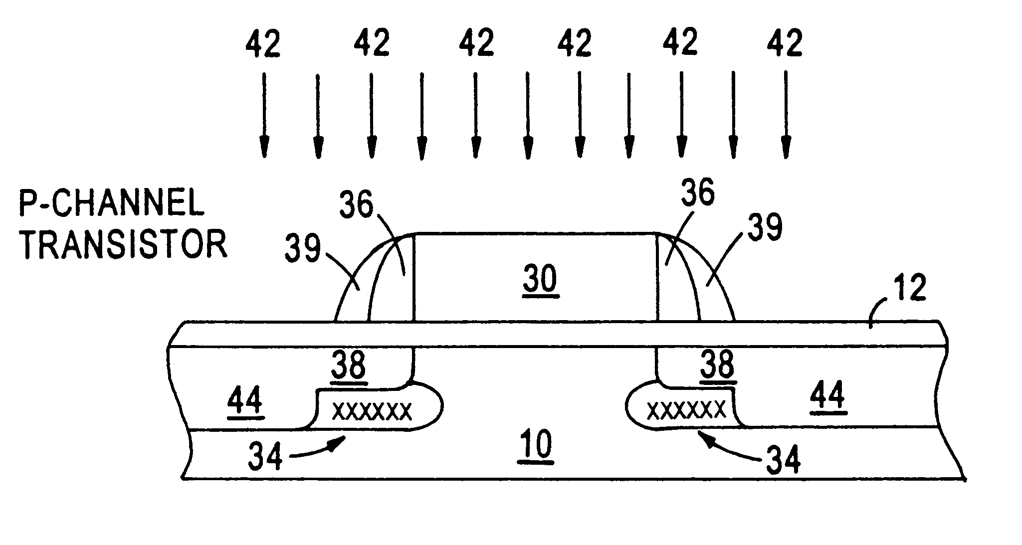
The present invention provides methodology enabling the manufacture of semiconductor devices exhibiting significantly reduced susceptibility to short channel effects while achieving high production throughput. In accordance with the present invention, halo implant regions are formed at zero degree tilt angles, thereby reducing the number of process steps and saving manufacturing time vis-a-vis conventional practices employing large angle tilt implants.

The present invention also provides methodology enabling control of the junction depth (X.sub.J) of a P-channel transistor independently of the X.sub.J of an N-channel transistor and provides greater independent control of the respective lengths of the channel regions of the P-channel and N-channel transistors.

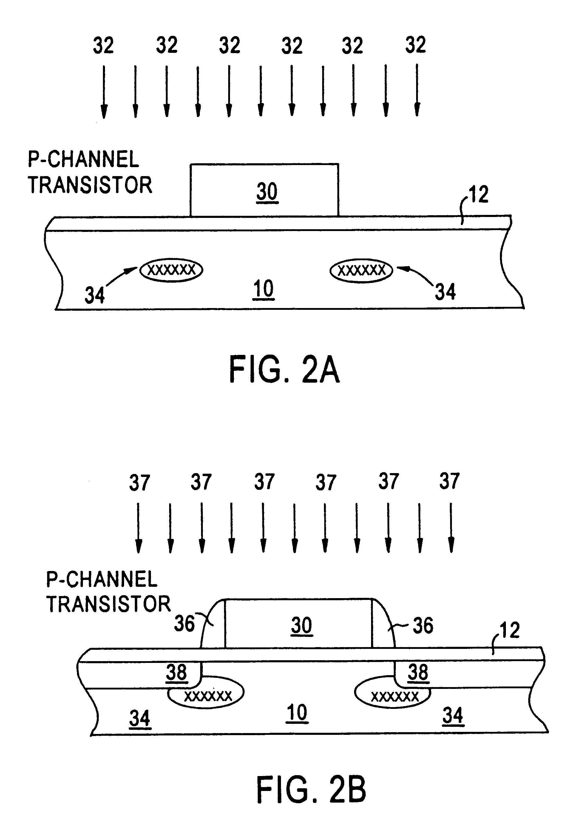
An embodiment of the present invention is schematically illustrated in FIGS. 2A through 2C. Adverting to FIG. 2A, a gate dielectric layer 12, such as silicon oxide, is formed on semiconductor substrate 10, typically comprising do...


PUM


Abstract

Halo implant regions are formed in a P-channel semiconductor device employing a zero degree tilt angle. N-type impurities are ion implanted to the desired depth in the semiconductor substrate prior to forming P-channel lightly doped source / drain areas. Subsequently, moderately or heavily doped source / drain regions are formed, followed by activation annealing. The halo implants diffuse to form halo structures at the desired location, thereby reducing short channel effects, such as subsurface punchthrough. Other embodiments enable independent control of the junction depths and channel lengths of N- and P-channel transistors, while maintaining high manufacturing throughput.

Description

CROSS REFERENCE TO THE RELATED APPLICATIONSThe subject matter involved in this application is related to the subject matter involved in commonly-assigned, co-pending application Ser. No. 08 / 924,640, filed Sep. 5, 1997, now U.S. Pat. No. 5,943,565 issued on Aug. 24, 1999, entitled CMOS PROCESSING EMPLOYING SEPARATE SPACERS FOR INDEPENDENTLY OPTIMIZED TRANSISTOR PERFORMANCE.1. Technical FieldThe present invention relates to a method of manufacturing a semiconductor device with improved reliability and increased manufacturing throughput. The invention has particular applicability in manufacturing high density CMOS semiconductor devices with design features of 0.25 microns and under.2. Background ArtThe escalating requirements for high density and performance associated with ultra large scale integration semiconductor devices require design features of 0.25 microns and under, such as 0.18 microns and under, increased transistor and circuit speeds, high reliability and increased manufact...

Claims


Application Information

Patent Timeline
Patent Type & Authority Patents(United States)
IPC IPC(8): H01L21/70H01L21/336H01L21/02H01L21/8238
CPCH01L21/823807H01L21/823814H01L29/66537H01L29/6656H01L29/6659
Inventor JU, DONG-HYUKLUNING, SCOTT
Owner GLOBALFOUNDRIES INC
Why Eureka
Try Eureka