Liquid crystal display device

a display device and liquid crystal technology, applied in the direction of instruments, static indicating devices, etc., can solve the problems of deterioration of contrast, response of liquid crystal, extreme deformation of contrast, etc., and achieve the effect of high contrast and linear gray scale display characteristic, facilitating gray shade display control operation

Inactive Publication Date: 2001-05-15
CITIZEN WATCH CO LTD
View PDF12 Cites 19 Cited by
  • Summary
  • Abstract
  • Description
  • Claims
  • Application Information

AI Technical Summary

Benefits of technology

Accordingly, a problem to be solved by the present invention is to provide an antiferroelectric liquid crystal display device that institutes measures for preventing an occurrence of a change in the mean value of the optical transmittance of liquid crystals during the holding time period tk, thereby stabilizing a black display state and facilitating a gray shades display control operation and realizing a high-contrast with linear-gray scale display characteristic.

Problems solved by technology

The main cause of this is the responsivity of the liquid crystal.
When actually driven, it is difficult to bring such a liquid crystal panel into a complete antiferroelectric state, and a dark display cannot be effected and that the contrast is extremely degraded.
Therefore, it is found that this phenomenon results not only in deterioration in the contrast but also in gradual increase in the mean value of the optical transmittance during the holding period tk even in the case of displaying halftone gray scale and that there is caused a serious problem in that a linear-gray shades display cannot be obtained.

Method used


Image

  • Liquid crystal display device
  • Liquid crystal display device
  • Liquid crystal display device

Examples


first embodiment

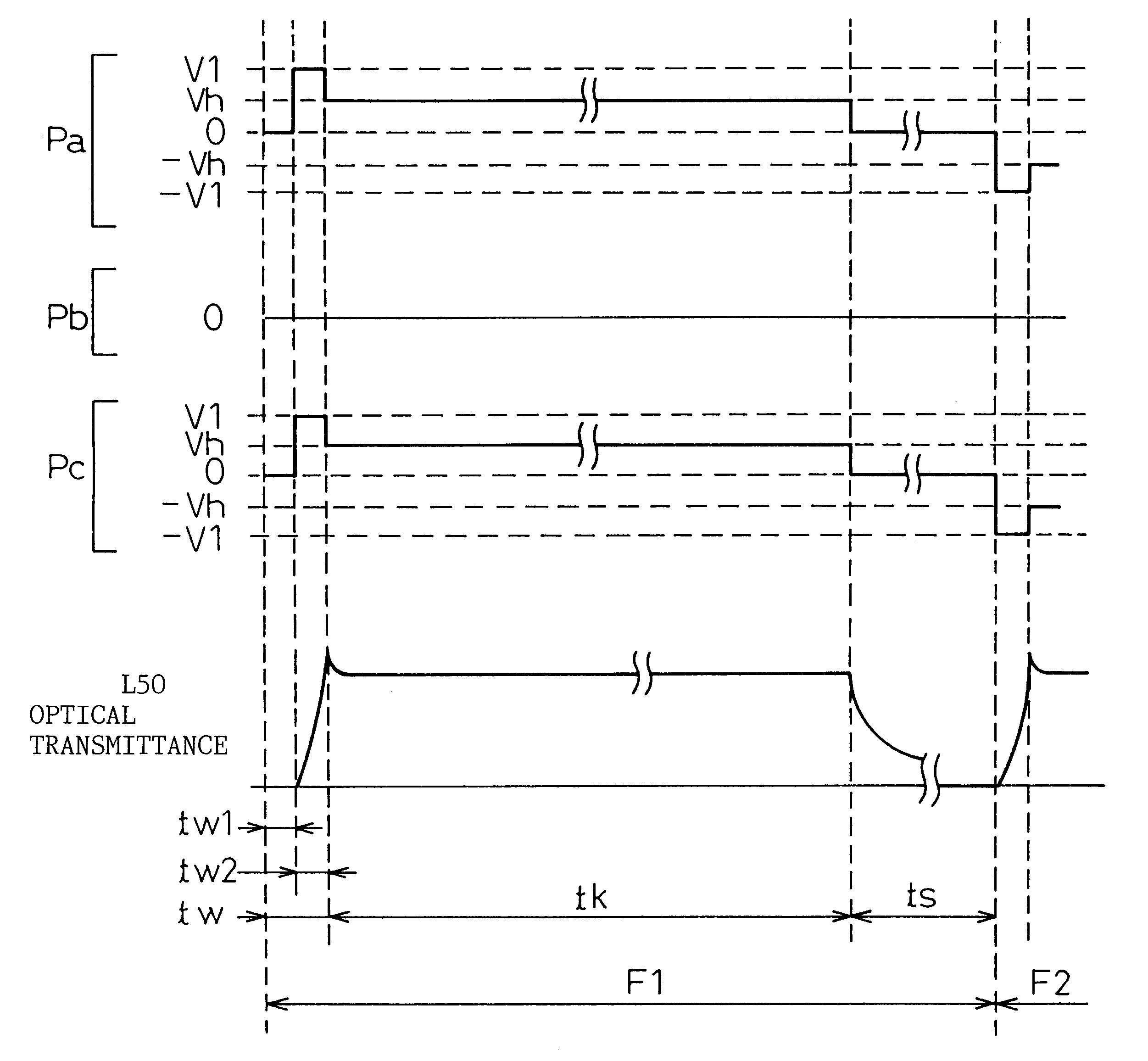
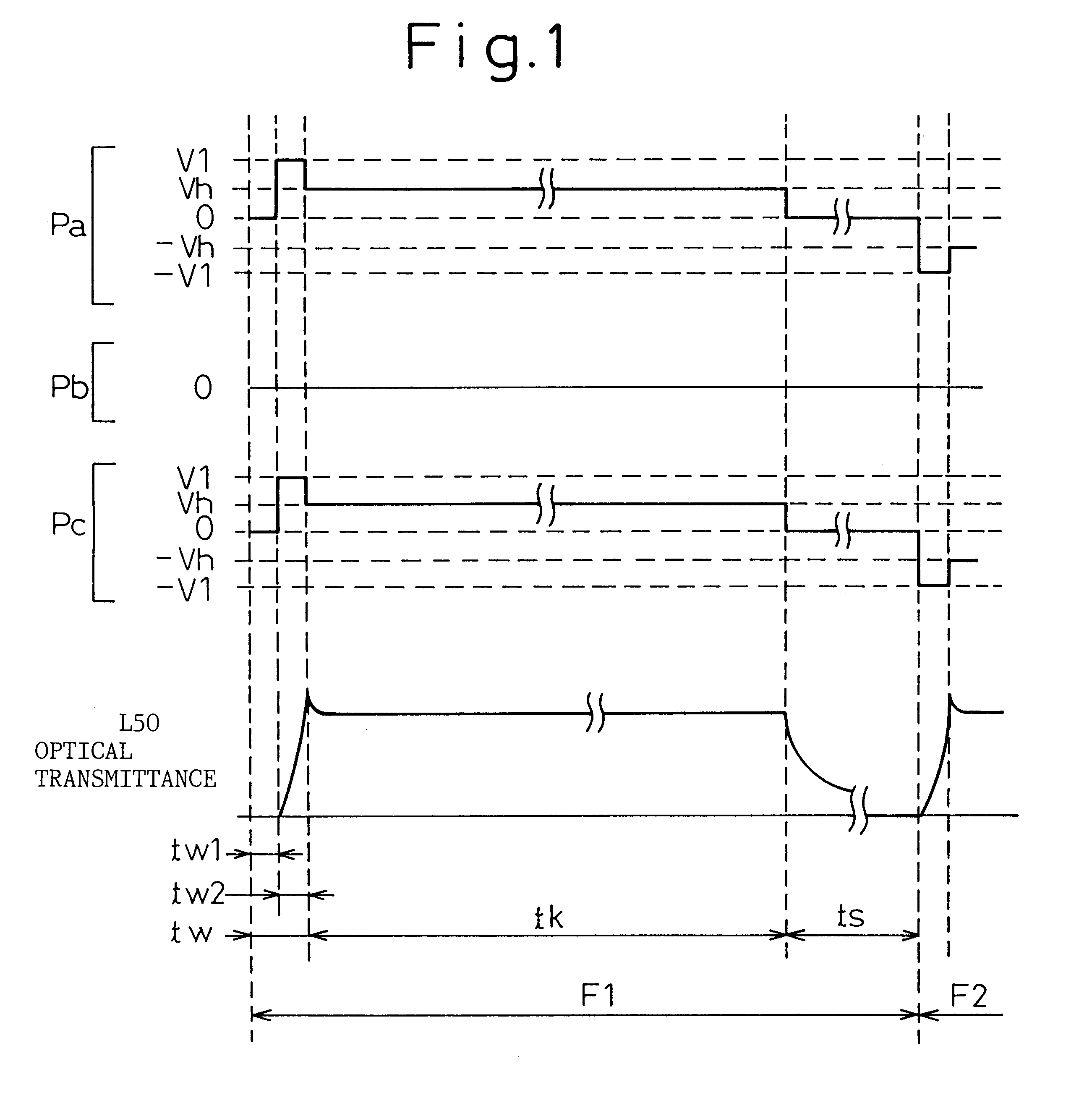
FIG. 1 illustrates the driving waveforms concerning pixels of interest and further illustrates change in the optical transmittance in the case of the present invention. Further, FIG. 1 is a diagram showing the waveform (Pa) of a scanning signal, the waveform (Pb) of a display signal, the waveform (Pc) of a synthesis voltage to be applied to a given pixel of interest, and the optical transmittance L50. Moreover, FIG. 1 illustrates the case that the aforementioned first measure was performed when all pixels on a column electrode, to which the pixel of interest belongs, are in a halftone gray scale state. In this case, this embodiment obtained gray scale levels by performing an amplitude modulation method. Here, when tw1 and tw2 denote a first half and a second half of the selection period tw, respectively, the voltage level, which is represented by each signal in the time periods tw1, tw2, the holding period tk and the relaxation period ts in the first frame, is as listed hereinbelow....

second embodiment

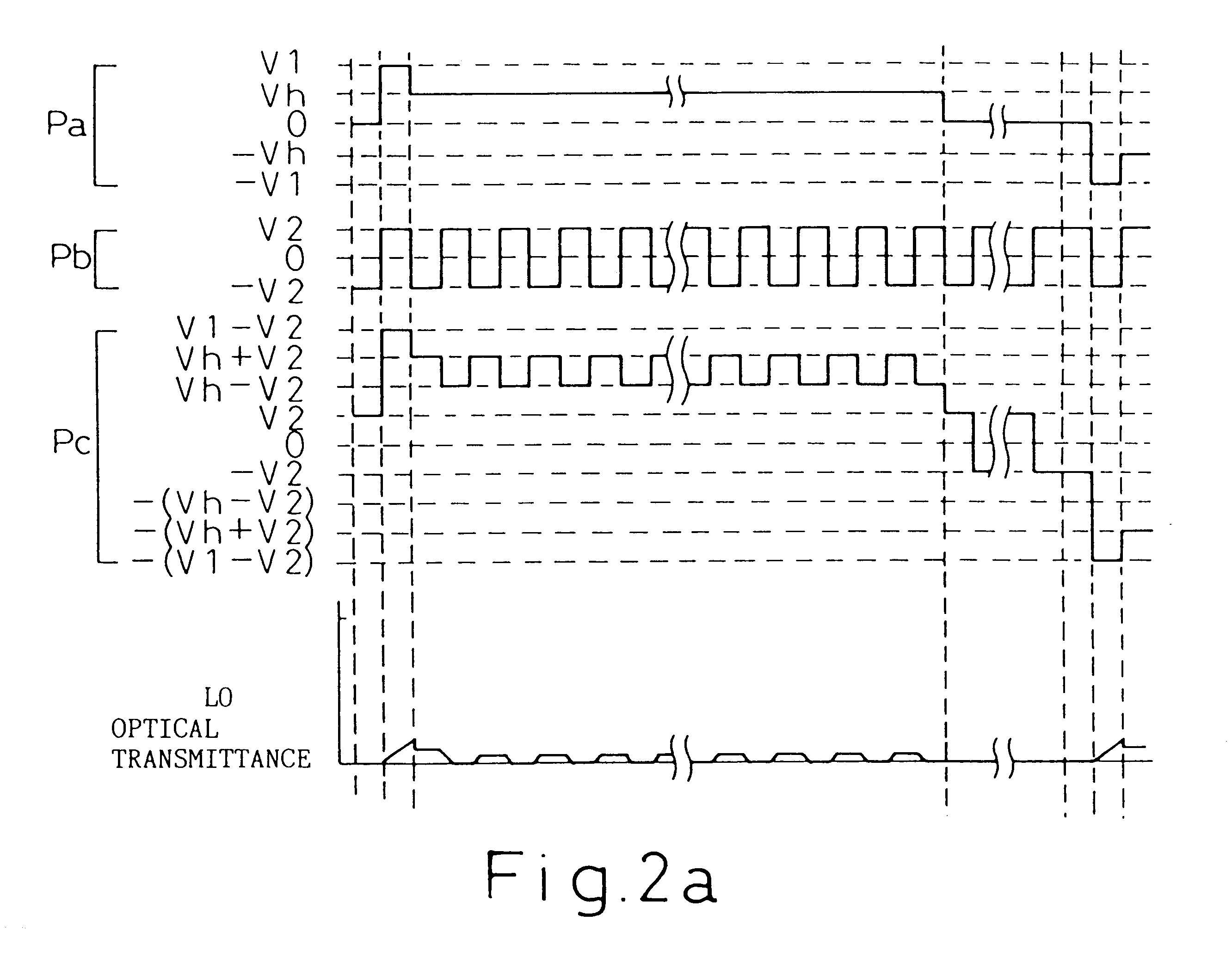
FIG. 2 is a diagram illustrating the driving waveform concerning a pixel of interest and further illustrates change in the optical transmittance in the case of the present invention. FIG. 2(a) illustrates the case that the aforementioned second measure is performed when all pixels on a column electrode, to which the pixel of interest belongs, are in a dark state. In this case, when tw1 and tw2 denote a first half and a second half of the selection period tw, respectively, the voltage level, which is represented by each signal in the time periods tw1, tw2, the holding period tk and the relaxation period ts in the first frame F1, is as listed hereinbelow.

Incidentally, the voltage of the display signal is set in such a manner that .vertline.Vh+V2.vertline.<.vertline.Ft.vertline.. In the case of the liquid crystal panel used in this embodiment, the value Vh is closed to the value At. As a result, the following inequality holds: .vertline.Vh-V2.vertline.<.vertline.At.vertline..

In the cas...

third embodiment

FIG. 3 illustrates the present invention and shows the driving waveform and the optical transmittance in the case of the performing the gray shades display by utilizing the pulse width modulation. Incidentally, it is assumed that all of the pixels other than a pixel of interest on a same column electrode are in the bright state. In the case illustrated by FIG. 3(a), it is assumed that the display signal voltage in the selection period tw of the first frame is (-V2) in (tw1-j) which is a leading part of the period tw1, and V2 in j which is the remaining part of the period tw1, that the display signal voltage is V2 in (tw2-j) which is a leading part of the period tw2, and (-V2) in j which is the remaining part of the period tw2. Namely, in the time period tw2, a time period, in which the voltage (V1+V2) is applied to the liquid crystal, is j which is the time period. Thus, the gray scale is displayed by controlling each of the voltages and changing the length j in such a manner that t...


PUM


Abstract

An antiferroelectric liquid crystal display device provided with means for preventing optical transmittance or the mean value of the optical transmittance from changing in a holding period tk. Thereby, the black display state thereof is stabilized. Further, the control of a gray shades display is facilitated. Moreover, linear gray scale characteristics and high contrast are provided. Thus, in the antiferroelectric liquid crystal display device having a selection period tw and the holding period tk, the optimum holding voltage (Vh), by which the optical transmittance little changes in the holding period tk, is applied to liquid crystals.

Description

The present invention relates to a liquid crystal display device using an antiferroelectric liquid crystal display panel that has a plurality of columns electrodes and a plurality of row electrodes.An antiferroelectric liquid crystal is stable in an antiferroelectric state when left in a condition that no voltage (zero) is applied to the liquid crystal. Hereinafter, this stable state will be referred to as a neutral state. An antiferroelectric liquid crystal panel may be configured in such a manner as to effect either a dark display or a bright display in this neutral state. Although antiferroelectric liquid crystal panels of the present invention be applied to both a dark display and a bright display, an antiferroelectric liquid crystal panel which is adapted to effect a dark display in the neutral state will be described hereinbelow.FIG. 7 is an example of a graph illustrating the optical transmittance of an antiferroelectric liquid crystal relative to a voltage applied thereto. I...

Claims


Application Information

Patent Timeline
Patent Type & Authority Patents(United States)
IPC IPC(8): G09G3/36G09G3/20
CPCG09G3/3633G09G3/2007G09G3/2011G09G3/2014G09G2310/061G09G2320/041
Inventor IMOTO, SATOSHIEBIHARA, HEIHACHIRO
Owner CITIZEN WATCH CO LTD
Why Eureka
Try Eureka