Semiconductor device having deposited silicon regions and a method of fabrication

a silicon region and semiconductor technology, applied in the direction of semiconductor devices, basic electric elements, electrical equipment, etc., can solve the problems of source/drain contact resistance negatively affecting device performance, undesired redistribution of dopants, and the structure and method of conventional mos transistor fabrication cannot be simply "scaled down" to produce smaller transistors for higher density integration

Inactive Publication Date: 2001-05-22
INTEL CORP
View PDF9 Cites 311 Cited by
  • Summary
  • Abstract
  • Description
  • Claims
  • Application Information

AI Technical Summary

Problems solved by technology

Unfortunately, the structure and method of fabrication of conventional MOS transistors cannot be simply "scaled down" to produce smaller transistors for higher density integration.
As device features are continually scaled down, the source / drain contact resistance negatively impacts device performance.
Unfortunately, present techniques for selectively depositing silicon generally require high temperature hydrogen predeposition bakes at 900.degree. C. or higher for a period of a minute or longer.
Such high temperature predeposition bakes increase the thermal energy seen by the devices which can cause an undesired redistribution of dopants.
As such, one is presently unable to selectively deposit a silicon film onto p-type and n-type silicon surfaces at the same time.
Still further, present processing techniques are unable to uniformly deposit highly (>5.times.10.sup.2 l atoms / cm.sup.3) insitu doped silicon films at a low temperatures and with a low thermal budget without discontinuities or faceting, making present deposition techniques incompatible with the formation of raised source / drain regions.

Method used


Image

  • Semiconductor device having deposited silicon regions and a method of fabrication
  • Semiconductor device having deposited silicon regions and a method of fabrication
  • Semiconductor device having deposited silicon regions and a method of fabrication

Examples


Embodiment Construction

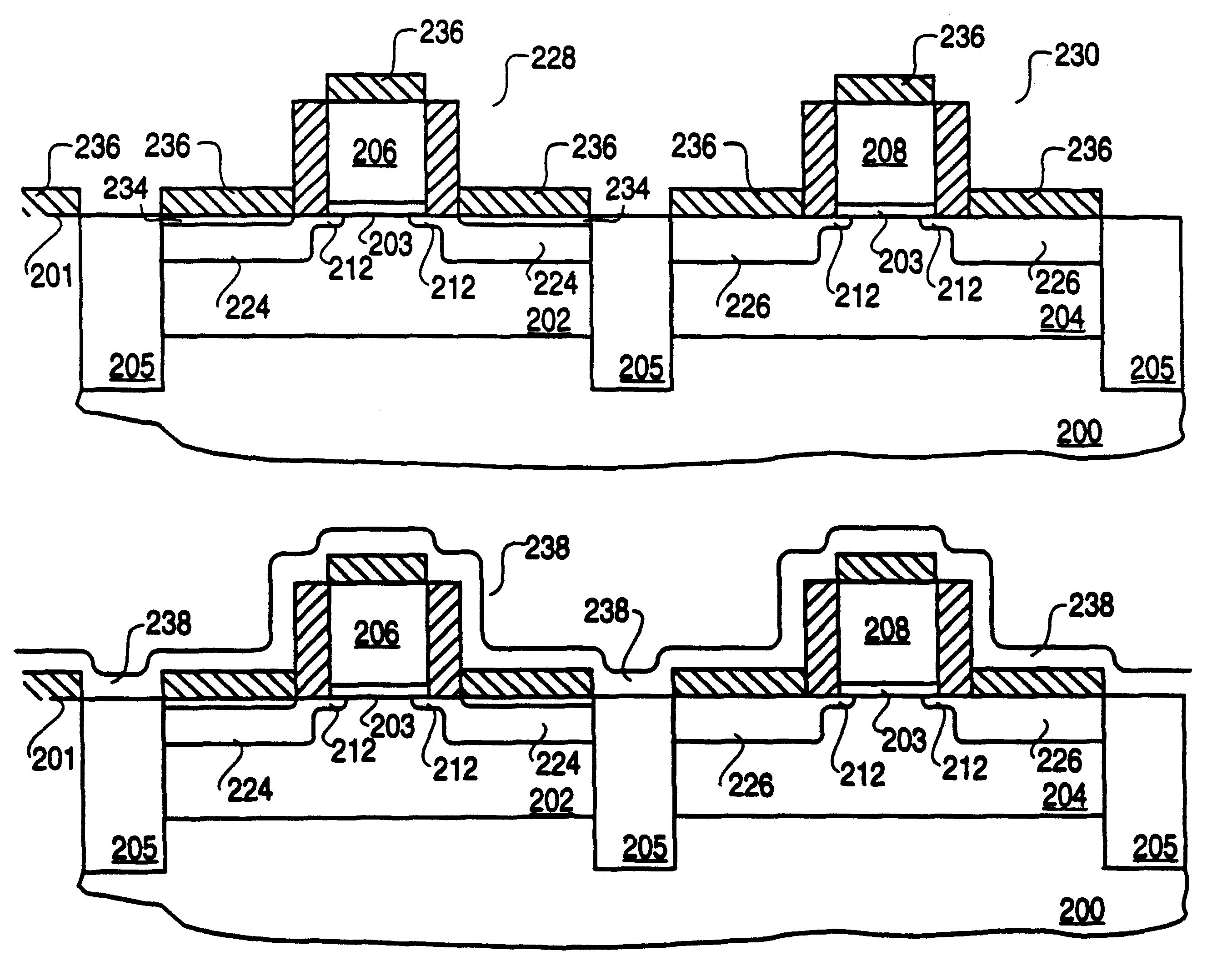
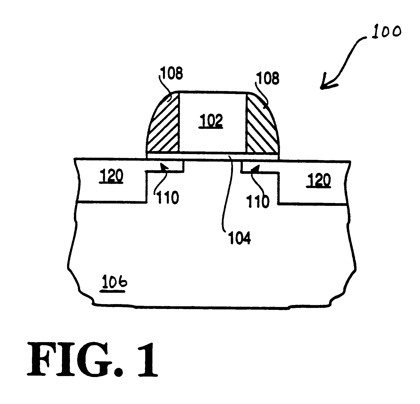
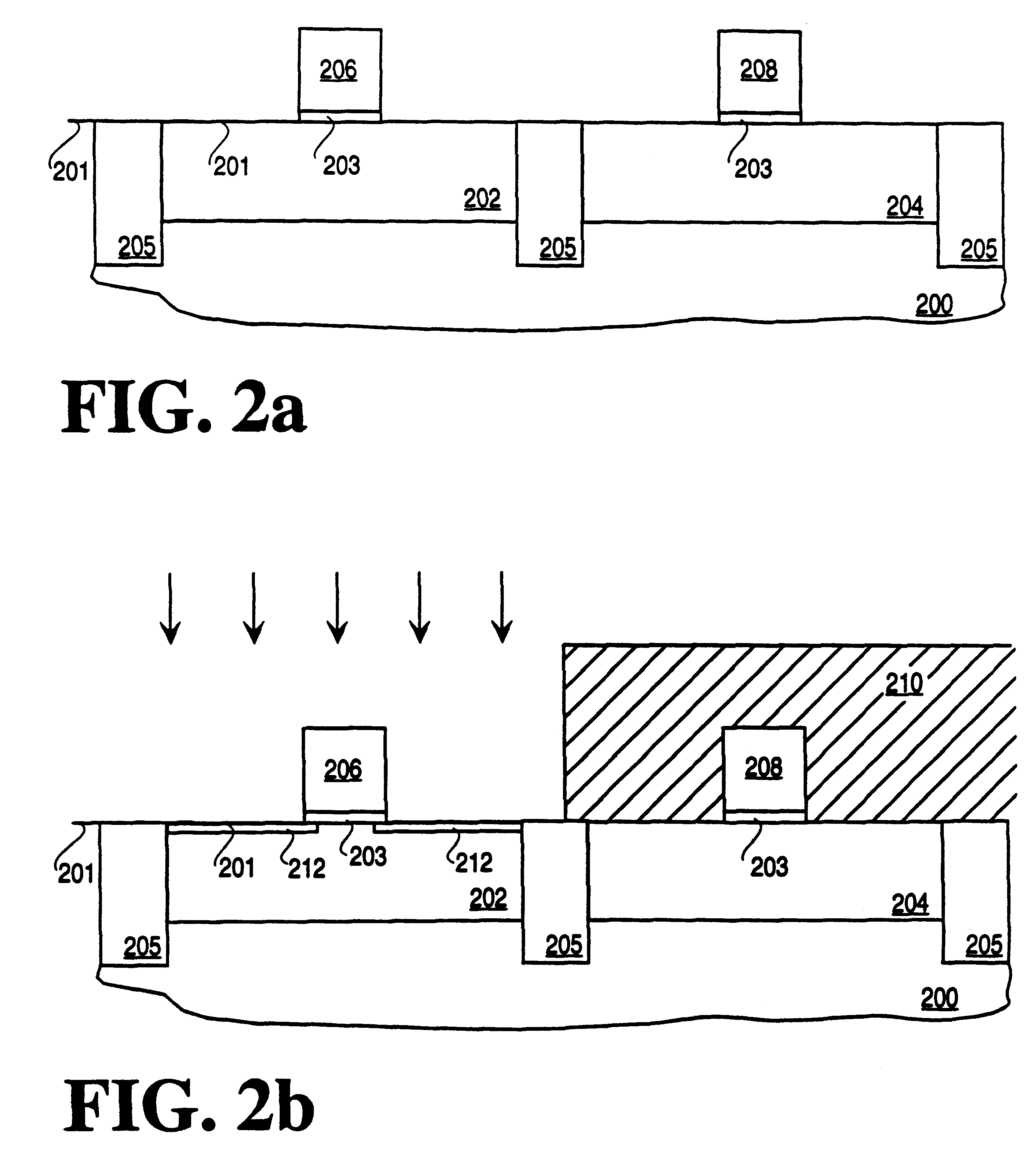
The present invention describes a novel semiconductor device having deposited silicon regions and methods of fabrication. In the following description numerous specific details are set forth, such as specific materials, dimensions, and processes etc., in order to provide a thorough understanding of the present invention. It will be obvious, however, to one skilled in the art that the invention may be practiced without the specific details. In other instances, well known semiconductor equipment and processes have not been described in particular detail in order to avoid unnecessarily obscuring the present invention.

The present invention is ideally suited for forming a pair of complementary metal oxide semiconductor (CMOS) devices. Standard processing techniques are used to form a pMOS device and nMOS device on a semiconductor substrate. A very low energy implant is then used to deposit n-type dopants into the surface of the p-type source / drain regions of the pMOS device or alternativ...


PUM

PropertyMeasurementUnit
temperatureaaaaaaaaaa

Abstract

The present invention describes an MOS device having deposited silicon regions and its a method of fabrication. In one embodiment of the present invention a substrate having a thin oxide layer formed on a silicon surface is heated and exposed to an ambient comprising germane (GeH4) to remove the thin oxide from the silicon surface. A silicon or silicon alloy film can then be deposited onto the silicon surface of the substrate.

Description

1. Field of the InventionThe present invention relates to the field of semiconductor manufacturing and more specifically to a method of forming a novel MOS transistor with deposited silicon regions.2. Discussion of Related ArtToday literally millions of individual transistors are coupled together to form very large-scale integrated (VSLI) circuits, such as microprocessors, memories, and application specific integrated circuits (IC's). Presently, the most advanced IC's are made up of approximately three million transistors, such as metal oxide semiconductor (MOS) field effect transistors having gate lengths on the order of 0.25 .mu.m. In order to continue to increase the complexity and computational power of future integrated circuits, more transistors must be packed into a single IC (i.e., transistor density must increase). Thus, future ultra large-scale integrated (ULSI) circuits will require very short channel transistors with effective gate lengths less than 0.1 .mu.m. Unfortunat...

Claims


Application Information

Patent Timeline
Patent Type & Authority Patents(United States)
IPC IPC(8): H01L21/70H01L21/8238
CPCH01L21/823814H01L21/823842H01L29/41783
Inventor MURTHY, ANANDJAN, CHIA-HONGANDIDEH, EBRAHIMWELDON, KEVIN
Owner INTEL CORP
Why Eureka
Try Eureka