Chip layout for implementing arbitrated high speed switching access of pluralities of I/O data ports to internally cached DRAM banks and the like

a technology of i/o data ports and dram banks, which is applied in the direction of digital storage, memory adressing/allocation/relocation, instruments, etc., can solve the problems of not being able to achieve extremely high switching speeds, prior chip layout schemes are not suited to accommodating the operation, etc., and achieve high efficiency and economic

Inactive Publication Date: 2001-05-22
NEXABIT NETWORKS
View PDF5 Cites 52 Cited by
  • Summary
  • Abstract
  • Description
  • Claims
  • Application Information

AI Technical Summary

Benefits of technology

A primary object of the present invention, accordingly, is to provide a new and improved chip layout particularly designed for implementing said multi-port internally cached DRAM bank high speed switching techniques and the like, and in a highly efficient and economical manner.

Problems solved by technology

Prior chip layout schemes have not, however, been suited to accommodating the operation and extremely high switching speeds and other quite different characteristics of the above-mentioned Chatter, universal multi-port internally cached DRAM bank operation.
In such, wherein there is provided a switching module logic control for connecting any of the I / O resources through serial interfaces with any I / O resource buffer competing for access to a common bus under a dynamic configuration of switching allocation appropriate for the desired data routability among the interfaces--with the switching module assigning any buffer to any serial interface and without any intermediate step of data transfer--prior chip layout schemes have not been suited to accommodating this operation and the extremely high switching speeds attainable therewith.

Method used


Image

  • Chip layout for implementing arbitrated high speed switching access of pluralities of I/O data ports to internally cached DRAM banks and the like
  • Chip layout for implementing arbitrated high speed switching access of pluralities of I/O data ports to internally cached DRAM banks and the like

Examples


Embodiment Construction

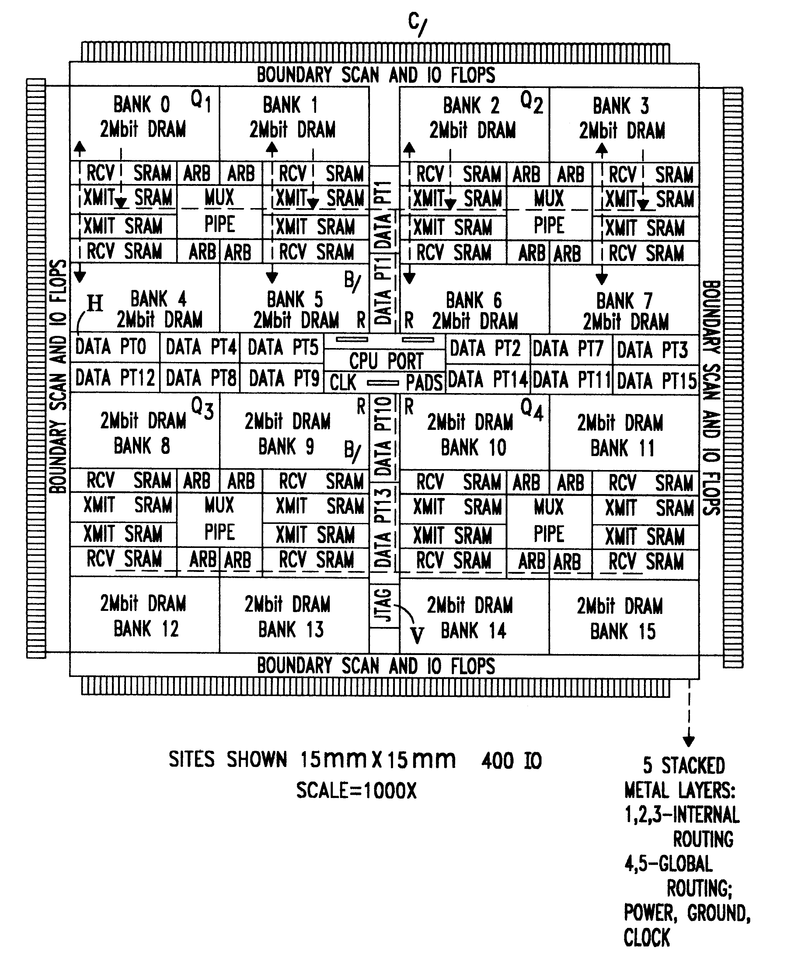
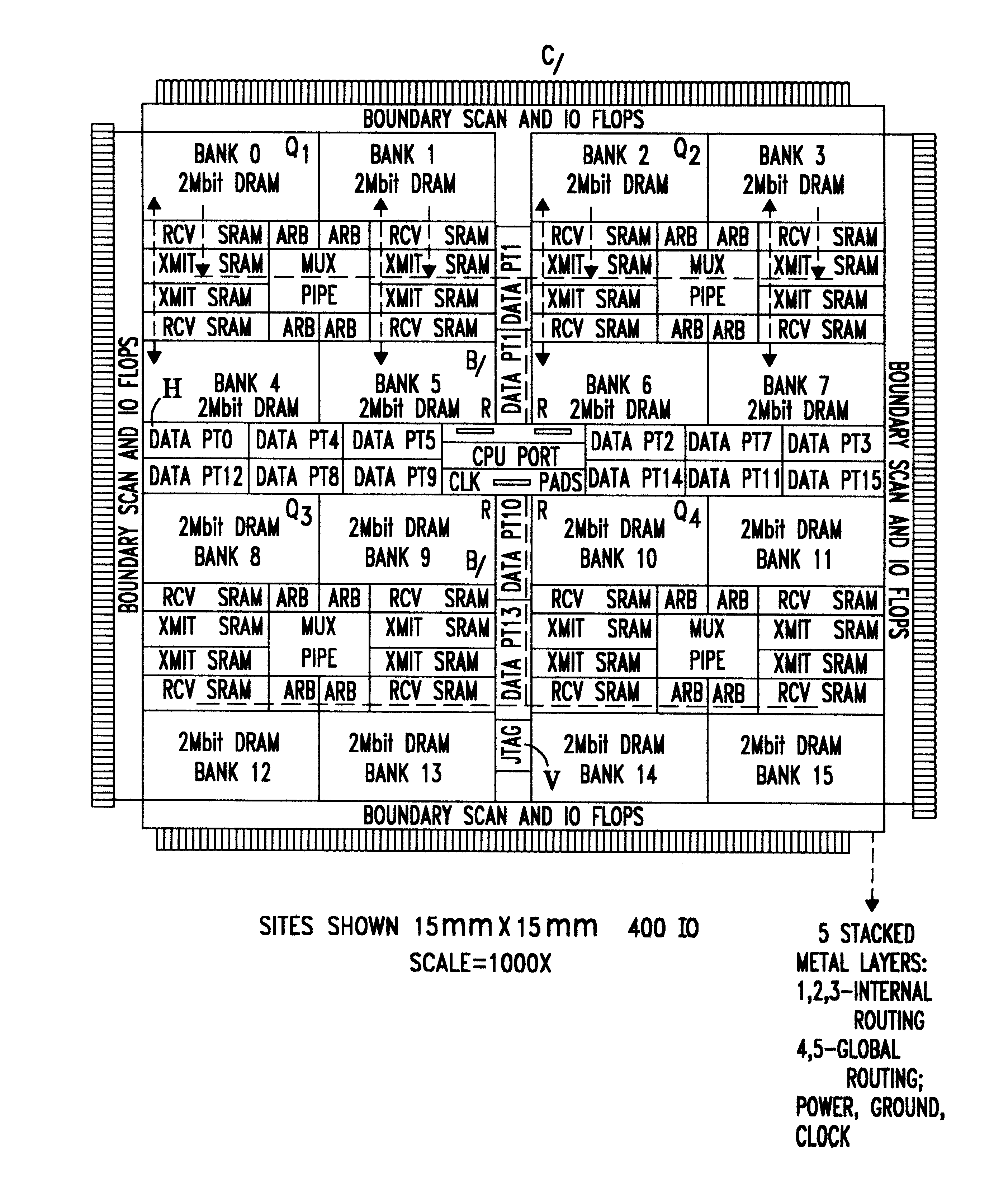
As may be gathered from the previous description, the invention is primarily directed to a chip layout particularly tailored for networks wherein pluralities of I / O data ports are each connected to buffer banks, as of the transmit / receive static RAM or SRAM type, operable under arbitration units to access pluralities of internally cached DRAM banks via internal busses to enable switching data connections at very high speeds amongst all the data ports through serial interfaces with any of the buffers under a dynamic switching allocation configuration. In the Chatter technology, external CPU or similar external data port control is useful, though internal control may also be employed, all as described in detail in the cited Chatter documents, above.

The drawing shows a preferred layout or "floor plan" for the above components as used in the Chatter system; it being understood that all the detailed circuit connections described in said documents and known and understandable by those ski...


PUM


Abstract

A novel chip layout for a network wherein pluralities of I/O data ports are each connected to transmit/receive SRAM buffer banks operable under arbitration units to access pluralities of internally cached DRAM banks via internal busses to enable switching data connections amongst all data ports through the appropriate buffers, the chip layout having, data ports substantially symmetrically placed with each data port connected to each arbitration unit and each transmit/receive buffer bank, and with each data port enabled to write into any DRAM bank, with the connections being effected such that each data port is substantially symmetric with respect to DRAM bank, arbitration unit and transmit/receive buffer banks and busses; and with timing clocks centrally placed on the chip to minimize clock skew by symmetric clock distribution.

Description

The present invention relates to microelectronic chips for enabling high speed I / O data port communication with network DRAM banks, and the like, being more particularly, though not exclusively, directed to chip layouts particularly tailored for operation with the universal multi-port internally cached DRAM bank high speed switching techniques described in Mukesh Chatter U.S. Pat. No. 5,799,209 and published in PCT publication document WO97 / 24725.Many approaches have been used for the layout of various types of network switching and communication chips. Prior chip layout schemes have not, however, been suited to accommodating the operation and extremely high switching speeds and other quite different characteristics of the above-mentioned Chatter, universal multi-port internally cached DRAM bank operation. In such, wherein there is provided a switching module logic control for connecting any of the I / O resources through serial interfaces with any I / O resource buffer competing for ac...

Claims


Application Information

Patent Timeline
Patent Type & Authority Patents(United States)
IPC IPC(8): G11C5/02G06F12/08
CPCG11C5/025G06F12/0893
Inventor SOMAN, SATISHOPALKA, ZBIGNIEWCHATTER, MUKESH
Owner NEXABIT NETWORKS
Why Eureka
Try Eureka