

Flowable germanium doped silicate glass for use as a spacer oxide
a technology of germanium doped silicate glass and spacer oxide, which is applied in the direction of basic electric elements, electrical apparatus, and semiconductor devices, can solve the problems of retrograde wall profiles, difficult to remove the polysilicon that remains under the overhang portion of the insulating layer, and electrical shorts in the circuitry
- Summary
- Abstract
- Description
- Claims
- Application Information
AI Technical Summary
Problems solved by technology
Method used
Image

Examples
Embodiment Construction
Numerous specific details are set forth in the detailed description to provide a thorough understanding of the present invention. However, one of ordinary skill in the art, having the benefit of this disclosure, will understand that the present invention may be practiced without many of these details. One of ordinary skill will understand that many such details pertain only to a particular embodiment and that such details will be necessary or useful depending on the particular embodiment being employed. Conversely, in other instances, well known details have not been described in detail for the sake of clarity so as not to obscure the invention. It will be appreciated that supplying such details would be a routine undertaking for those of ordinary skill in the art, even if a complex and time-consuming task, given the benefit of this disclosure.
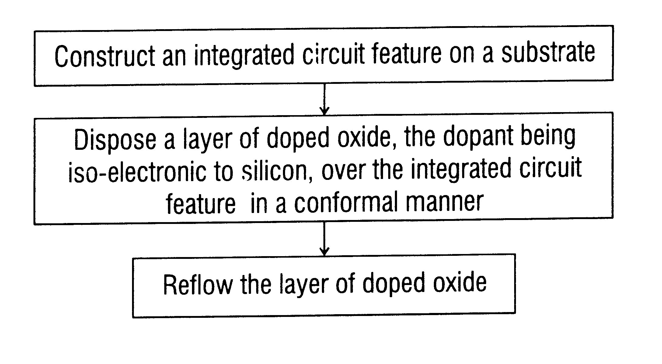
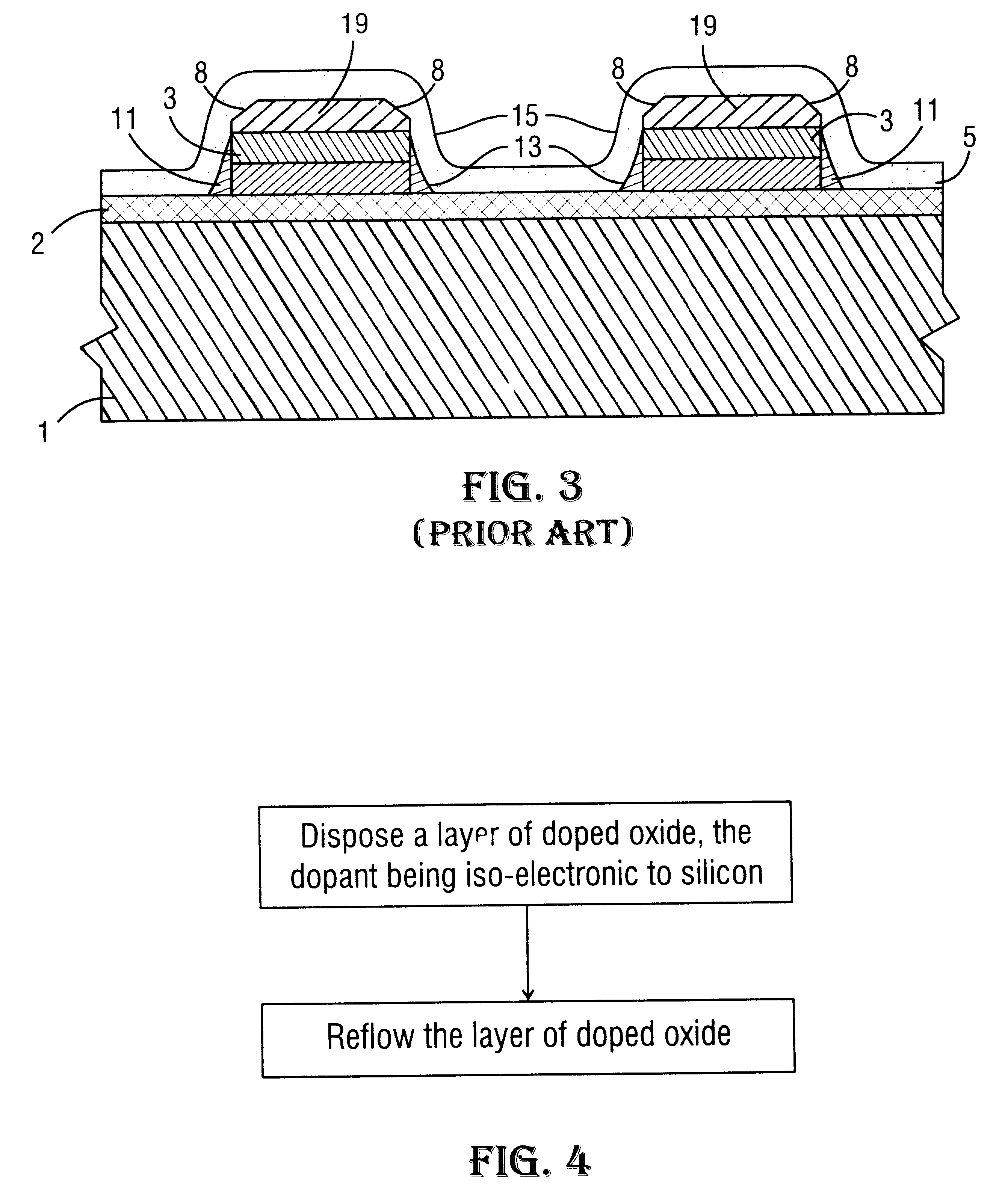
One embodiment of the present invention is diagrammed in FIG. 4 and may be generally described as a method for constructing an integrated cir...
PUM
 Abstract
Description
Claims
Application Information