Semiconductor memory

a technology of semiconductor devices and memory, applied in the field of semiconductor memory, can solve the problems of difficult process devices to meet such requirements, and achieve the effects of preventing poor yield, reducing the entire process cost, and prolonging the retention time of data

Inactive Publication Date: 2001-08-14
PANASONIC CORP
View PDF9 Cites 27 Cited by
  • Summary
  • Abstract
  • Description
  • Claims
  • Application Information

AI Technical Summary

Benefits of technology

Accordingly, an object of the present invention is to provide a longer data retention time for the realization of a longer refresh cycle period. Another object of the present invention is to prevent poor yields caused by short data retention times to achieve a reduction of the entire process cost.
In accordance with the present invention, the reference potential stored in a memory cell different from an information memory cell is designed to fall corresponding to a decrease in potential of the information memory cell due to a leakage of the signal charge, whereby a length of time, for the difference between the information potential and the reference potential to reach a sense limit, can be decreased. As a result, a longer data retention time is obtained.

Problems solved by technology

It seems hard for process devices to meet such requirements.

Method used


Image

  • Semiconductor memory
  • Semiconductor memory
  • Semiconductor memory

Examples


first embodiment

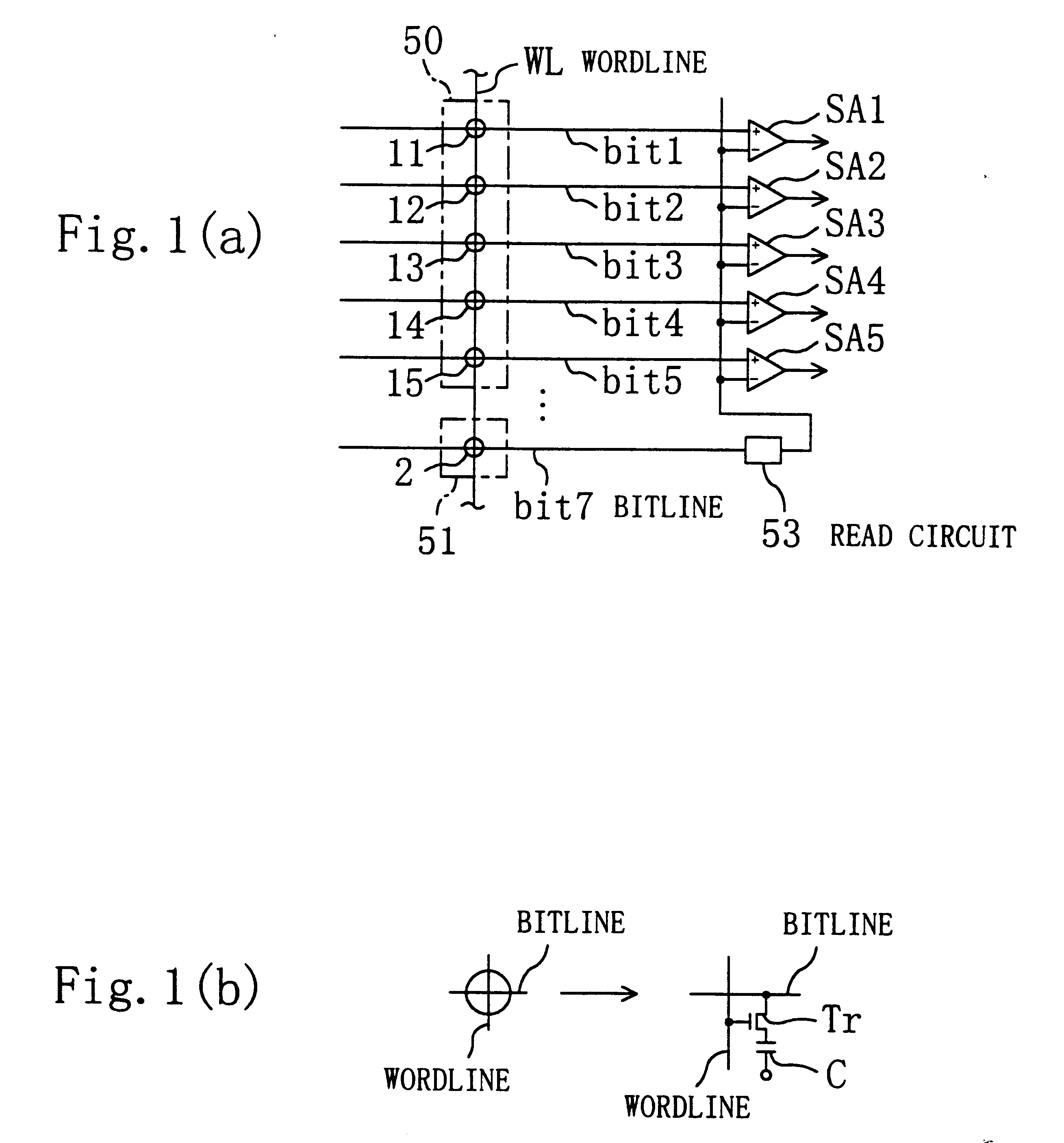
Referring first to FIG. 1, this invention is described.

In FIG. 1(a), 11-15 are memory cells (information memory cells) for storing information. These memory cells 11-15 belong in a first memory cell group 50. 2 is a memory cell that belongs in a second memory cell group 51. WL is a word line to which the memory cells 11-15 of the first memory cell group 50 and the memory cell 2 of the second memory cell group 51 are coupled. Each of the memory cells 11-15 and 2, shown in symbolic form in FIG. 1(a), is made up of a cell transistor Tr and a cell capacitor C as shown in detail in FIG. 1(b). In FIG. 1(b), only one word line WL is shown; however, there exist a plurality of word lines WL and memory cells 11-15 and 2 are coupled to a word line WL.

The memory cells 11-15 of the first memory cell group 50 are coupled, through bit lines bit1 to bit5, to differential input terminals of corresponding sense amplifiers SA1-SA5. On the other hand, the memory cell 2 of the second memory cell group 5...

second embodiment

Referring now to FIGS. 4 and 5, a second embodiment of the present invention is described below.

FIG. 4 shows the second embodiment. FIG. 5 illustrates in detail elements of the second embodiment.

In the second embodiment, the first memory cell group 50 is (vertically in the figure) divided into two sections and the second memory cell group 51 is disposed between these two sections. This arrangement aims to carry out reference potential information transmission from the second memory cell group 51 which stores reference potential information to the first memory cell group 50 in the same time with good symmetry and to allow the first and second memory cell groups 50 and 51 to receive the same amount of noise for noise cancellation.

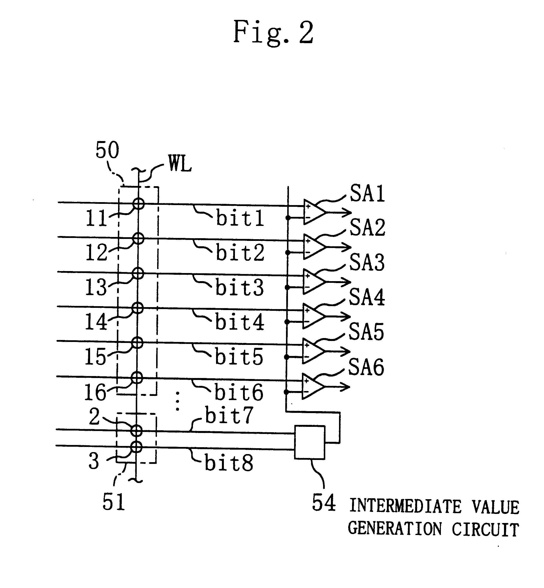
In the figure, in the second memory cell group 51 the number of reference memory cells coupled to the same word line is one. However, the FIG. 2 structure may be used. This, however, requires the provision of the intermediate value generation circuit 54.

In th...

third embodiment

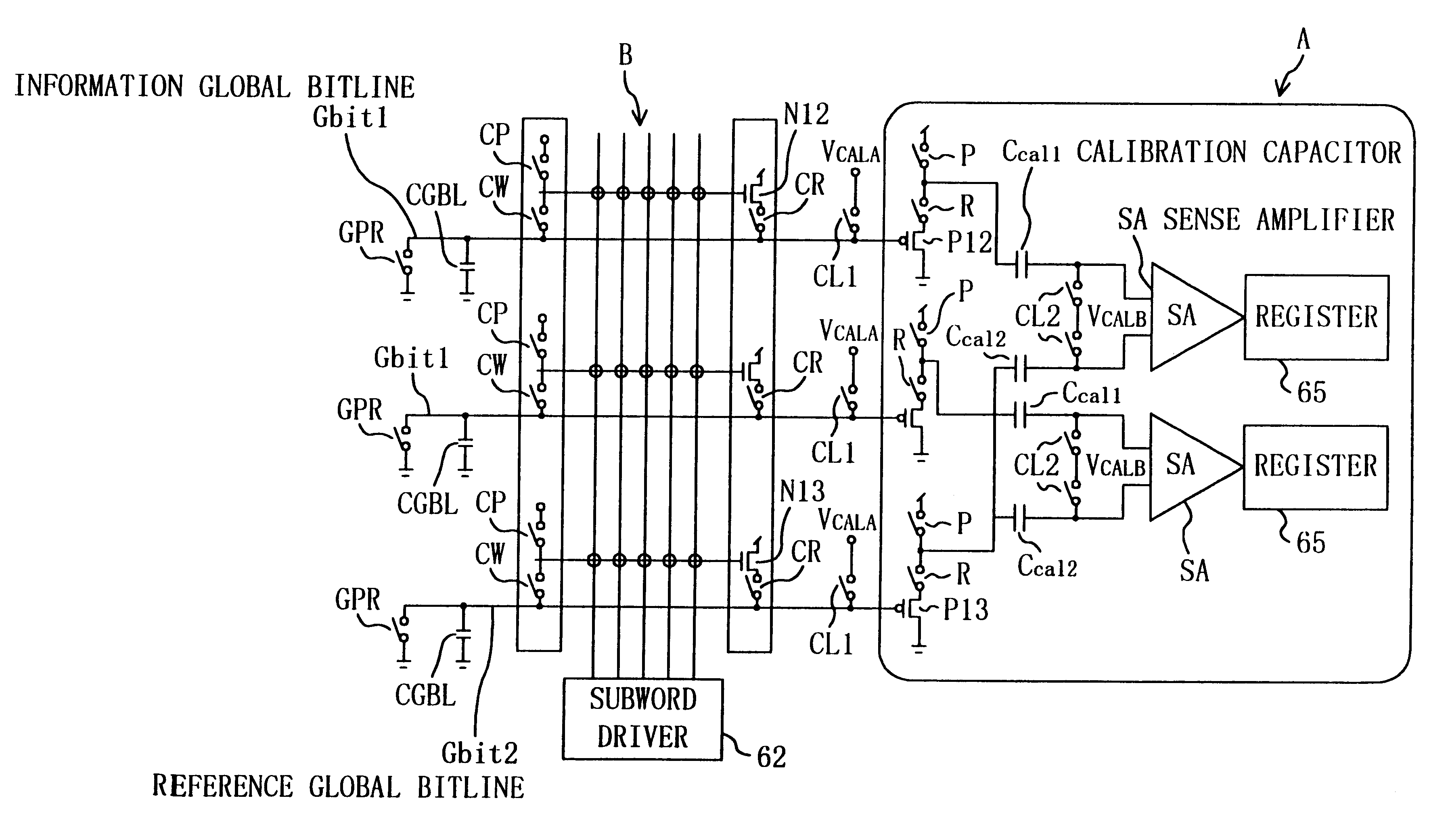
Referring now to FIGS. 8 and 9, a third embodiment of the present invention is described. The third embodiment is an improvement of the second embodiment.

The object of the present embodiment is to avoid the phenomenon, which takes place In the second embodiment, that there occurs a reduction in input voltage applied to the sense amplifier SA due to the signal propagation characteristic between the local probes PRBa and PRBb and variations in the signal propagation characteristic between the preamplification sections 60 and 61. The input voltage of the sense amplifier SA varies by a sum of the difference between the threshold voltages (Vtn) of the control transistors N12 and N22 of the two local probes and the difference between the threshold voltages (Vtp) of the control transistors P14 and P24, resulting in a decrease in operation margin. The present embodiment avoids the variation by means of calibration capacitors.

A calibration procedure is described below.

Referring to FIG. 9, bo...


PUM


Abstract

A plurality of information memory cells and a single reference memory cell are coupled to a single word line. The reference memory cell stores reference information equivalent to a reference potential to information readout. Pieces of information, stored in the information memory cells, are fed, over respective bit lines, to first input terminals of sense amplifiers. The reference information, stored in the reference memory cell, is fed, over a bit line, to second input terminals of the sense amplifiers. When the potential of signal charges stored in the information memory cells falls due to leakage current, the potential of a signal charge stored in the reference memory cell correspondingly falls due to leakage current. This prolongs a length of time taken for a difference between these potentials to reach a sense limit, thereby achieving a longer data retention time. As a result of such arrangement, even when there occurs a small current leakage from memory cells, it is possible to secure a long data retention time thereby making it possible to obtain a long refresh cycle period.

Description

BACKGROUND OF THE PRESENT INVENTIONThe present invention generally relates to the field of semiconductor memories. More particularly, the present invention relates to a DRAM and a memory core utilizable in embedded memories including DRAMs (dynamic random access memories) and logical circuits.The level of integration of memories, particularly the level of DRAM integration, has been improved increasingly year by year. In order to avoid a reduction of the serviceable time of memories, a longer refresh cycle period is required. The level of real performance values required for data retention times becomes higher. It seems hard for process devices to meet such requirements.Referring now to FIG. 23 the value of real performance of the memory data retention time will be described.FIG. 23 outlines a conventional DRAM. Cs is a storage capacitor in a DRAM memory cell. WL1 and WL2 are word lines. bit is a bit line and xbit is a bit line in complementary relationship with the bit line bit. Vpr...

Claims


Application Information

Patent Timeline
Patent Type & Authority Patents(United States)
IPC IPC(8): G11C11/4091G11C11/409G11C7/06G11C7/00G11C7/14G11C11/4099G11C11/406G11C29/00H01L27/108G11C11/401G11C29/04H01L21/8242H01L21/8246H01L27/10H01L27/105
CPCG11C7/062G11C7/14G11C11/406H01L27/10808G11C11/4099G11C29/785G11C11/4091H10B12/31
Inventor YAMADA, TOSHIOSHIBAYAMA, AKINORI
Owner PANASONIC CORP
Why Eureka
Try Eureka