Self-soldering integrated circuit probe assembly

a technology of integrated circuits and probes, which is applied in the direction of electronic circuit testing, measurement devices, instruments, etc., can solve the problems of difficult access to pins of ic mounted on circuit boards, difficult for a technician to simultaneously access more than one or two ic pins using this method, and difficult for such a probe to firmly grip the circuit board, etc., to achieve easy and firmly attached, easy to remove, and minimal load

Inactive Publication Date: 2001-09-11
CREDENCE SYSTEMS
View PDF5 Cites 12 Cited by
  • Summary
  • Abstract
  • Description
  • Claims
  • Application Information

AI Technical Summary

Benefits of technology

to provide a probe assembly that is easily and firmly attached to a flat pack or other type of integrated circuit package and thereafter easily removed, that low occupies little vertical space above the IC package, that presents a minimal load at the IC pins, and that minimizes the number of signal paths needed between the probe assembly and external test equipment.

Problems solved by technology

However it is difficult for a technician to concurrently access more than one or two IC pins using this method.
It is also often difficult to access pins of an IC mounted on a circuit board when the circuit board is in its normal operating environment.
However flat pack IC packages having pins that are soldered flush with the circuit board would be difficult for such a probe to firmly grip.
Also the described probe assembly is relatively tall and would not be useful where space above the IC is limited.
However the assembly is large and inconvenient to use insofar as the circuit board has to be mounted within the probe assembly rather than installed in its normal operating environment.
While this type of probe can grasp relatively thick integrated circuit packages, a flat pack package is typically so thin that it would be difficult for such a probe to firmly grip its body.
Also since the probe is held to an IC package body only by lateral pressure, it can easily fall off.
This probe assembly is also relatively tall and therefore not practical where space above the IC is limited.
However such a probe assembly would require a large number conductors to convey signals between the probe assembly and external test equipment requiring access to the IC pins.
However, since prior art probe assemblies provide a relatively long signal path between an IC pin and buffer amplifier, the capacitance and inductance of those signal paths act as a load on the IC pin.

Method used


Image

  • Self-soldering integrated circuit probe assembly
  • Self-soldering integrated circuit probe assembly
  • Self-soldering integrated circuit probe assembly

Examples


Embodiment Construction

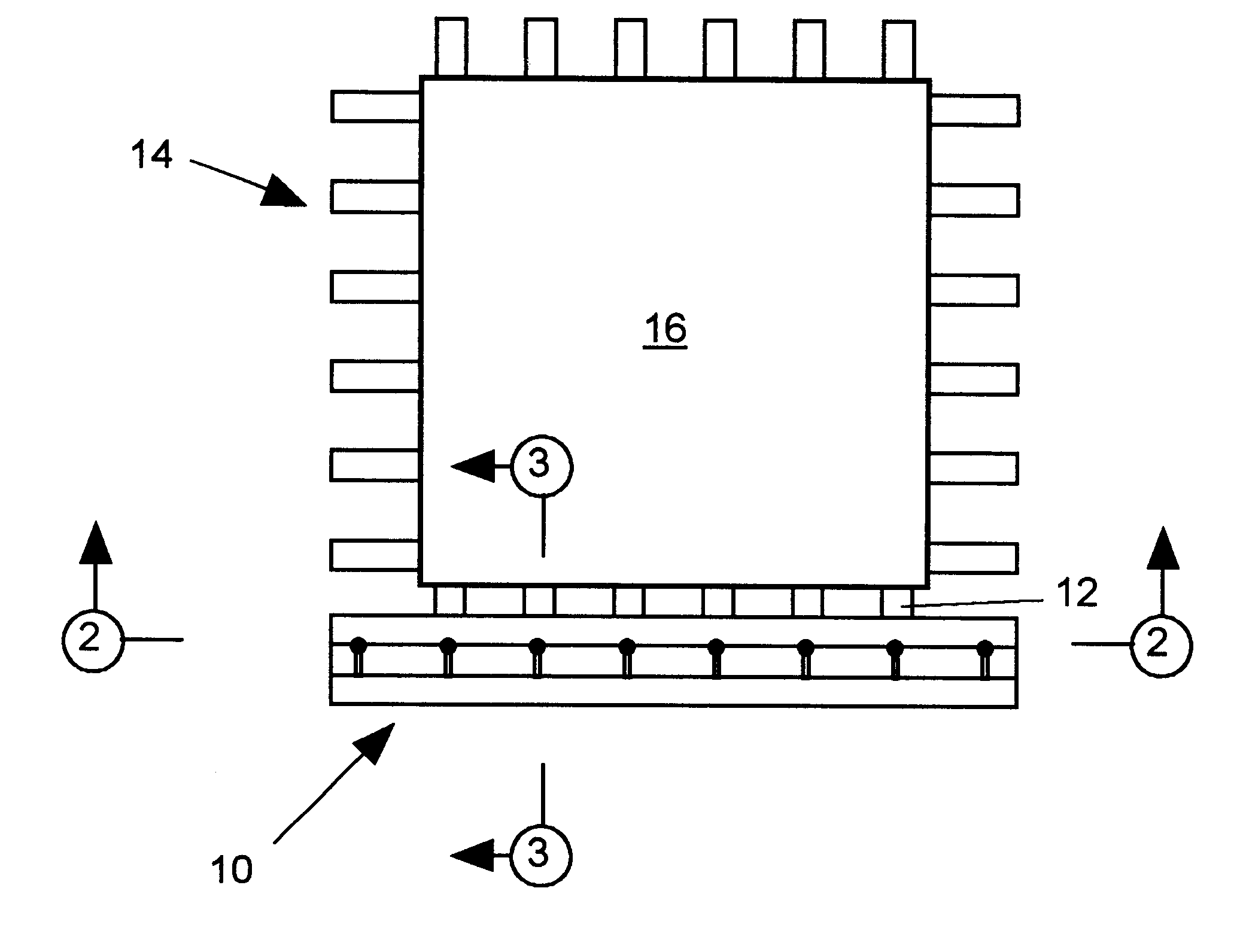
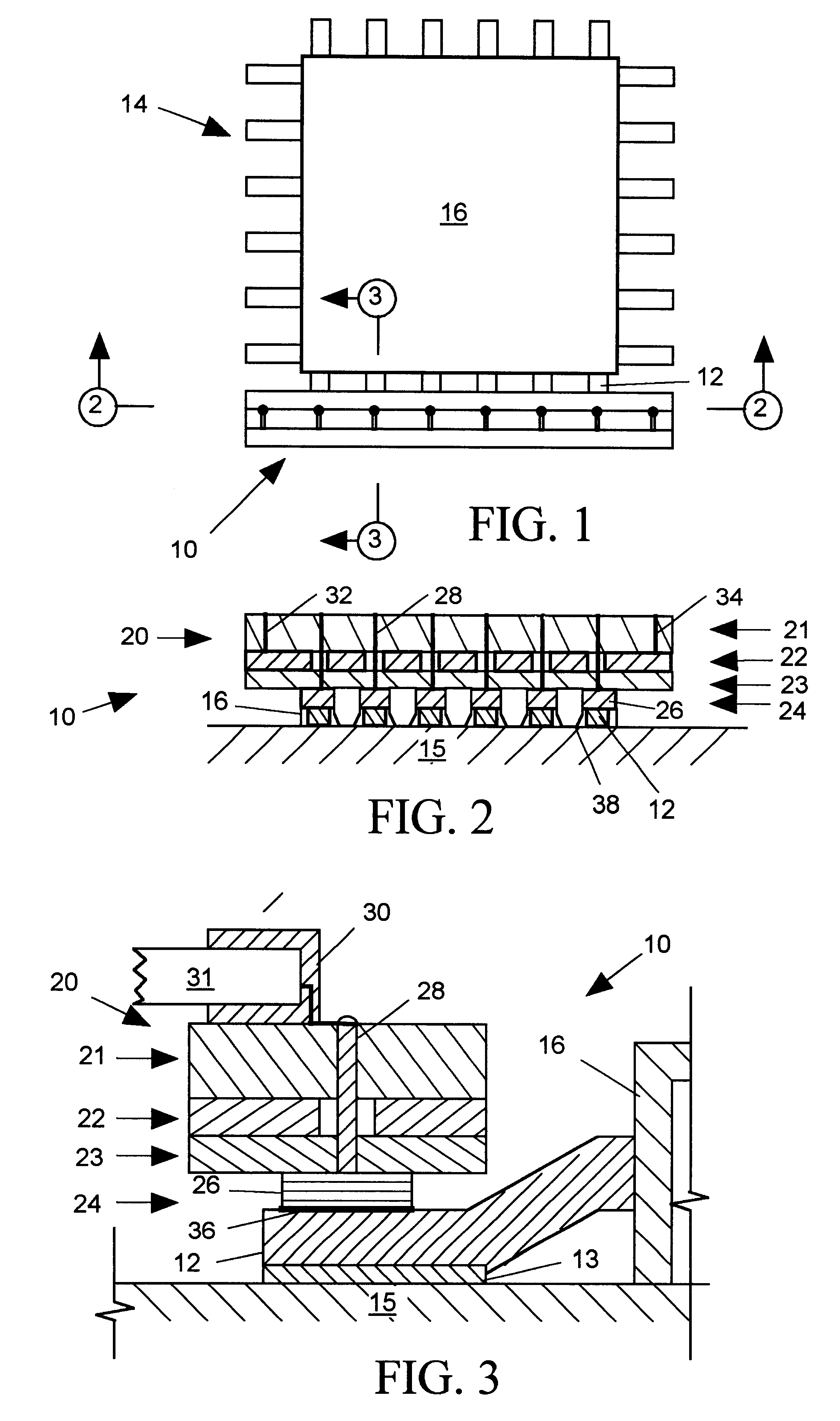
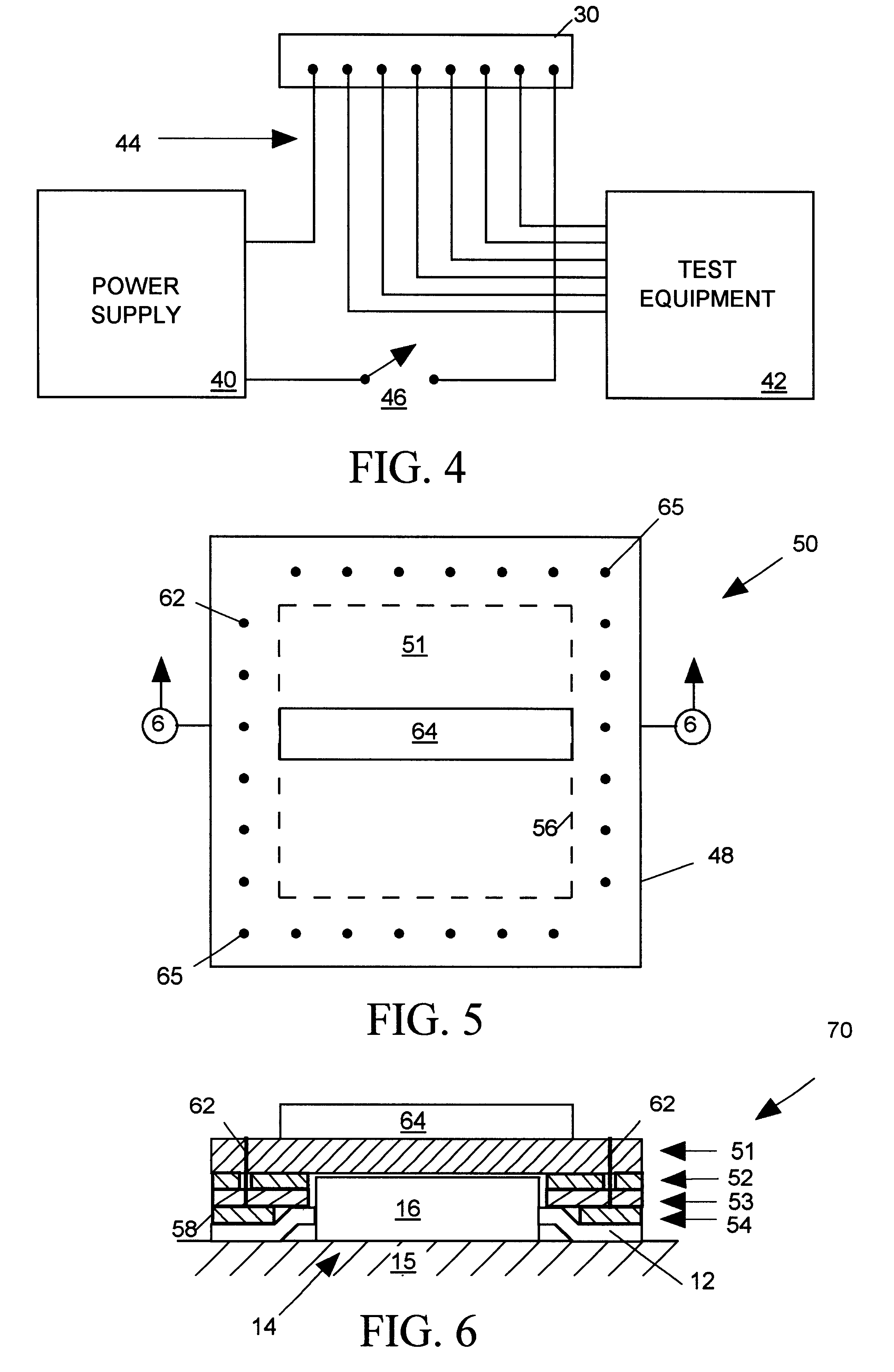
FIGS. 1-3 illustrate a probe assembly 10 in accordance with the invention for providing external test equipment with input / output signal access to a row of pins 12 of an integrated circuit (IC) package 14 soldered to pads 13 on the surface of a circuit board 15. Integrated circuit package 14 may be a conventional quad flat pack package as illustrated in FIG. 1 or may be any other type of IC package having a body 16 and at least one row of input / output pins 12 extending horizontally outward from body 16.

Probe assembly 10 includes a set of probes for providing signal paths for test equipment accessing pins 12. As described below, probe assembly 10 is designed so that it can be easily and firmly soldered in place over the IC package 14 and then easily removed. Probe assembly 10 is also designed to provide a relatively low vertical profile so that it can be used to access the pins of IC package 14 when relatively little space is available above the IC package 14. This makes probe assemb...


PUM


Abstract

A probe assembly for probing pins of an integrated circuit (IC) includes a base providing a set of solder-coated contacts arranged to contact a corresponding set of IC pins when the base is placed over the IC pins. The base also includes an heating element for briefly delivering heat to the contacts so that when the base is placed over the IC with the contacts in resting on the IC pins, the heat provided by heating element temporarily melts the solder coating on the contacts. Thereafter, the solder cools and solidifies to form a firm bond between the contacts to the IC pins. The heating element suitably comprises material that generates substantial heat in response to a voltage pulse applied across the heating element or alternatively may act as a heat conductor for conducting heat from an external heat source to the contacts.

Description

1. Field of the InventionThe present invention relates in general to integrated circuit (IC) probes and in particular to a self-soldering probe assembly that attaches a set of probes to input / output pins of a flat pack IC package.2. Description of Related ArtWhen testing a circuit implemented by integrated circuits (ICs) mounted on a circuit board, a technician can access a circuit node by manually holding a probe to a pin of an IC. However it is difficult for a technician to concurrently access more than one or two IC pins using this method. It is also often difficult to access pins of an IC mounted on a circuit board when the circuit board is in its normal operating environment. For example when the circuit board is installed in a backplane next to another circuit board there can be very little clearance between the circuit boards for accommodating a probe. Thus it would be beneficial to provide a probe that can be firmly connected to an IC mounted on a circuit board, that would r...

Claims


Application Information

Patent Timeline
Patent Type & Authority Patents(United States)
IPC IPC(8): G01R31/28
CPCG01R31/2886
Inventor WOHLFARTH, PAUL D.
Owner CREDENCE SYSTEMS
Why Eureka
Try Eureka