An etch stop layer for dual damascene process

a damascene and stop layer technology, applied in the direction of basic electric elements, semiconductor/solid-state device manufacturing, electric apparatus, etc., can solve the problems of difficult control of the depth of the timed etch step, the inability to work with traditional deposition/etch processes for forming interconnects, and the new problems of ic manufacturing processes

Inactive Publication Date: 2001-09-18
APPLIED MATERIALS INC
View PDF14 Cites 358 Cited by
  • Summary
  • Abstract
  • Description
  • Claims
  • Application Information

AI Technical Summary

Problems solved by technology

However, these materials present new problems for IC manufacturing processes.
For example, because copper is difficult to etch in a precise pattern, traditional deposition/etch processes for forming interconnects has become unworkable, and accordingly, a process referred to as a dual damascene is being used to form copper interconnects.
However, the depth of the timed etch s...

Method used


Image

  • An etch stop layer for dual damascene process
  • An etch stop layer for dual damascene process
  • An etch stop layer for dual damascene process

Examples


Embodiment Construction

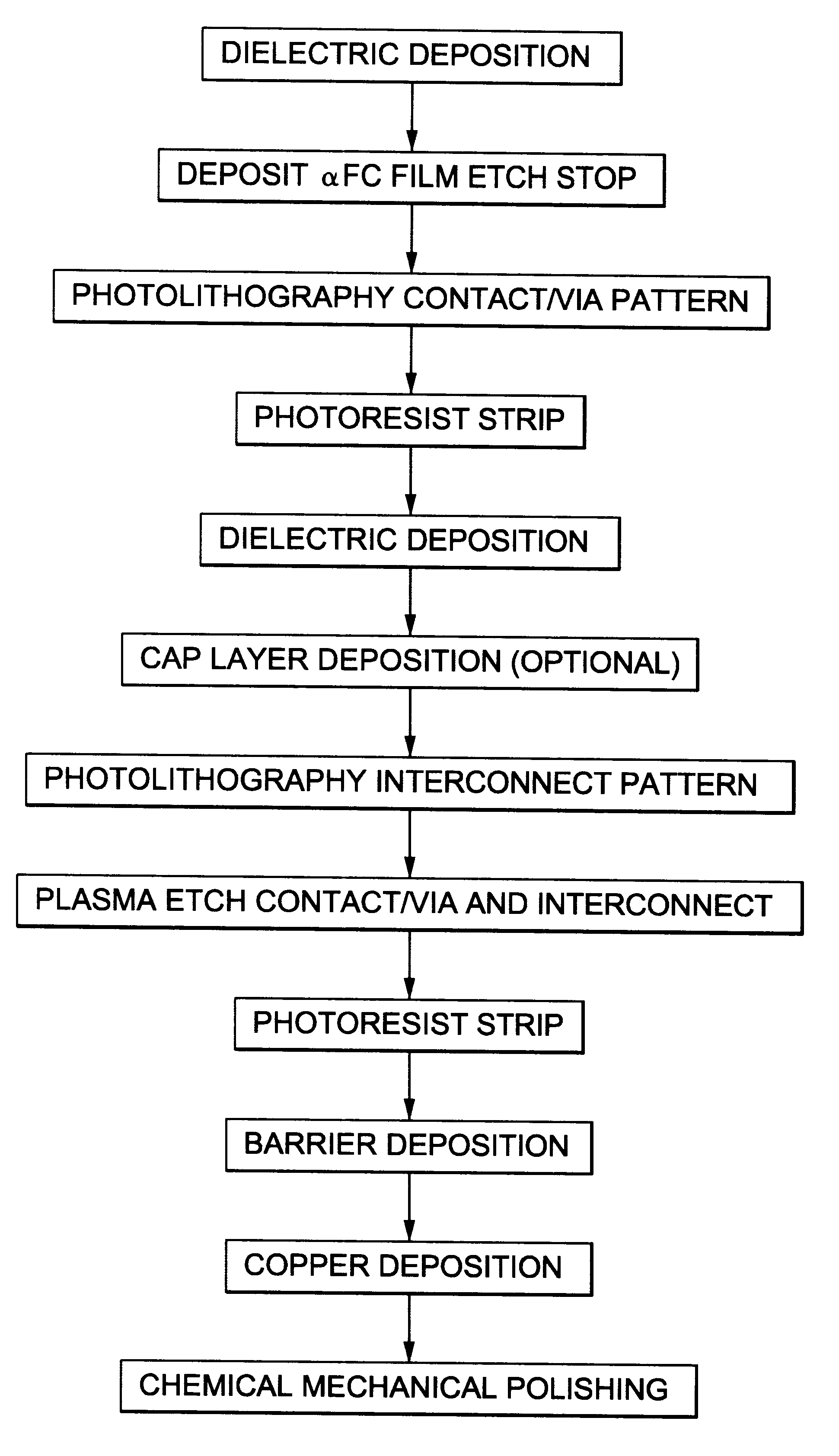
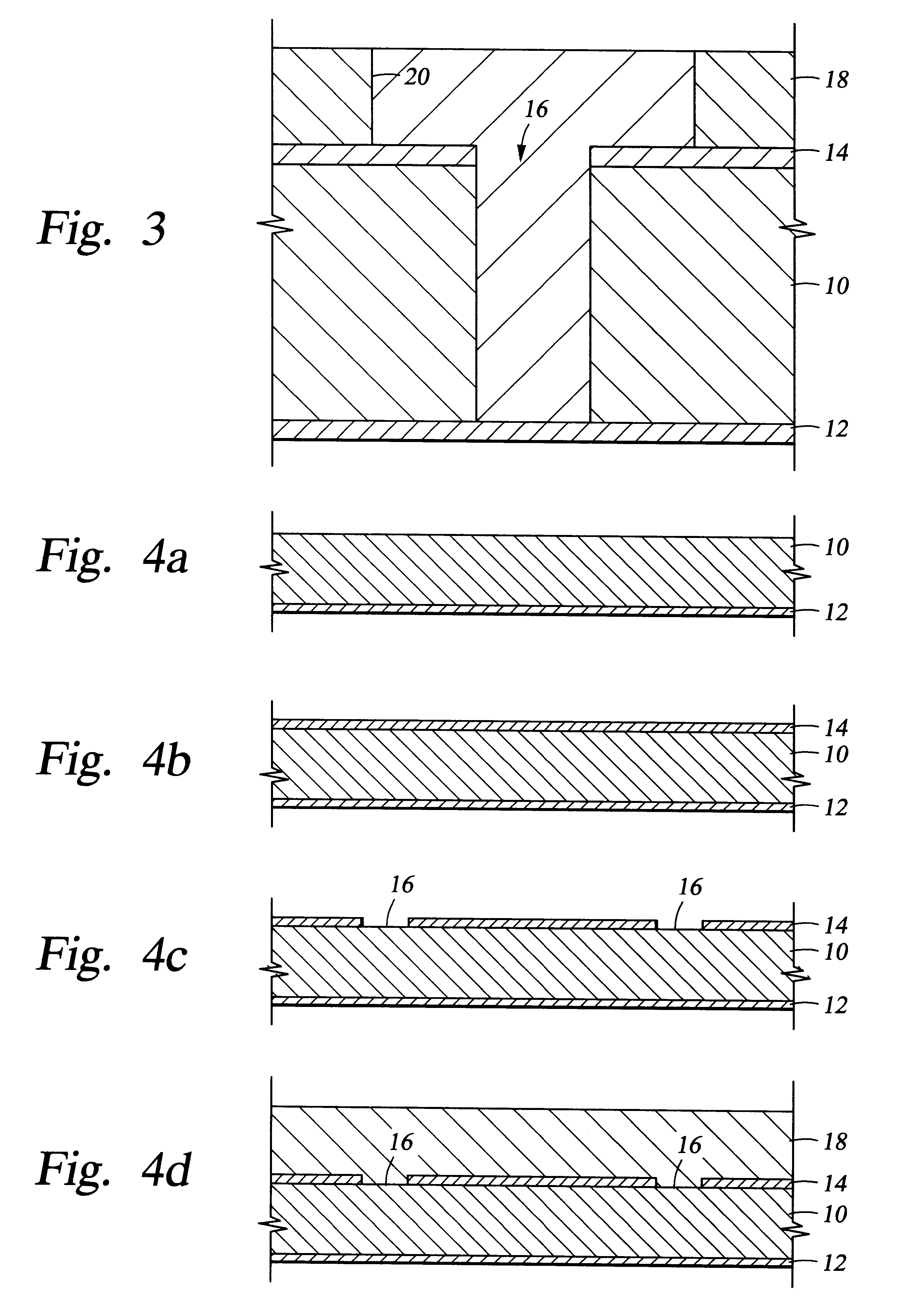
The present invention provides an improved dual damascene structure comprising a low k etch stop, preferably an amorphous, diamond-like carbon (.alpha.-C) material. Low k etch stop is defined herein as an etch stop having a dielectric constant equal to or lower than that of silicon nitride (dielectric constant .about.7.0). A dual damascene structure fabricated in accordance with the invention is shown in FIG. 4h and the method of making the structure is sequentially depicted schematically in FIGS. 4a-4h, which are cross sectional views of a substrate having the steps of the invention formed thereon.

As shown in FIG. 4a, an initial first dielectric layer 10, such as FSG, silicon oxide, or the like, is deposited on the substrate 12 to a thickness of about 5,000 to about 10,000 .ANG., depending on the size of the structure to be fabricated. As shown in FIG. 4b, a low k etch stop 14, such as .alpha.-C, .alpha.-FC, parylene, AF.sub.4, BCB, PAE, oxynitride or silicon carbide, is then depos...


PUM


Abstract

The present invention provides a carbon based etch stop, such as a diamond like amorphous carbon, having a low dielectric constant and a method of forming a dual damascene structure. The low k etch stop is preferably deposited between two dielectric layers and patterned to define the underlying interlevel contacts/vias. The second or upper dielectric layer is formed over the etch stop and patterned to define the intralevel interconnects. The entire dual damascene structure is then etched in a single selective etch process which first etches the patterned interconnects, then etches the contact/vias past the patterned etch stop. The etch stop has a low dielectric constant relative to a conventional SiN etch stop, which minimizes the capacitive coupling between adjacent interconnect lines. The dual damascene structure is then filled with a suitable conductive material such as aluminum or copper and planarized using chemical mechanical polishing.

Description

1. Field of the InventionThe present invention relates generally to the fabrication of integrated circuits on substrates. More particularly, the invention relates to a new etch stop layer and a process for forming a dual damascene structure characterized by a low capacitance between interconnect lines.2. Background of the InventionConsistent and fairly predictable improvement in integrated circuit design and fabrication has been observed in the last decade. One key to successful improvements is the multilevel interconnect technology which provides the conductive paths between the devices of an integrated circuit (IC) device. The shrinking dimensions of horizontal interconnects (typically referred to as lines) and vertical interconnects (typically referred to as contacts or vias: contacts extend to a device on the underlying substrate while vias extend to an underlying metal layer such as M1, M2, etc.) in very large scale integration (VLSI) and ultra large scale integration (ULSI) te...

Claims


Application Information

Patent Timeline
IPC IPC(8): H01L21/768H01L21/70
CPCH01L21/7681H01L21/76835H01L21/76829
Inventor SOMEKH, SASSON
Owner APPLIED MATERIALS INC
Why Eureka
Try Eureka