Quartz crystal microbalance sensors and semiconductor manufacturing process systems comprising same

a technology of quartz crystal microbalance and manufacturing process, applied in the field of sensors, can solve the problems of inability to realize real-time control, process inefficiency, and few available reliable and inexpensive methods to follow

Inactive Publication Date: 2001-10-02
LIFE SAFETY GERMANY
View PDF45 Cites 98 Cited by
  • Summary
  • Abstract
  • Description
  • Claims
  • Application Information

AI Technical Summary

Benefits of technology

to provide an improved semiconductor manufacturing

Problems solved by technology

Such lack of real-time control results in process inefficiencies.
Further, there are few available reliable and inexpensive methods to follow the progress of a reaction in the reaction vessel.
Such approaches have significant deficiencies in practice, however.
OES systems are prone to fogging of the optical windows employed in such systems, with consequent signal

Method used


Image

  • Quartz crystal microbalance sensors and semiconductor manufacturing process systems comprising same
  • Quartz crystal microbalance sensors and semiconductor manufacturing process systems comprising same
  • Quartz crystal microbalance sensors and semiconductor manufacturing process systems comprising same

Examples


Embodiment Construction

The disclosure of United States patent application Ser. No. 08 / 785,342 filed Jan. 17, 1996 in the names of Glenn M. Tom and Cynthia A. Miller for "Piezoelectric Sensor for Hydride Gases, and Monitoring Apparatus Comprising Same," and issued Oct. 27, 1998 as U.S. Pat. No. 5,827,947, is hereby incorporated herein by reference in its entirety.

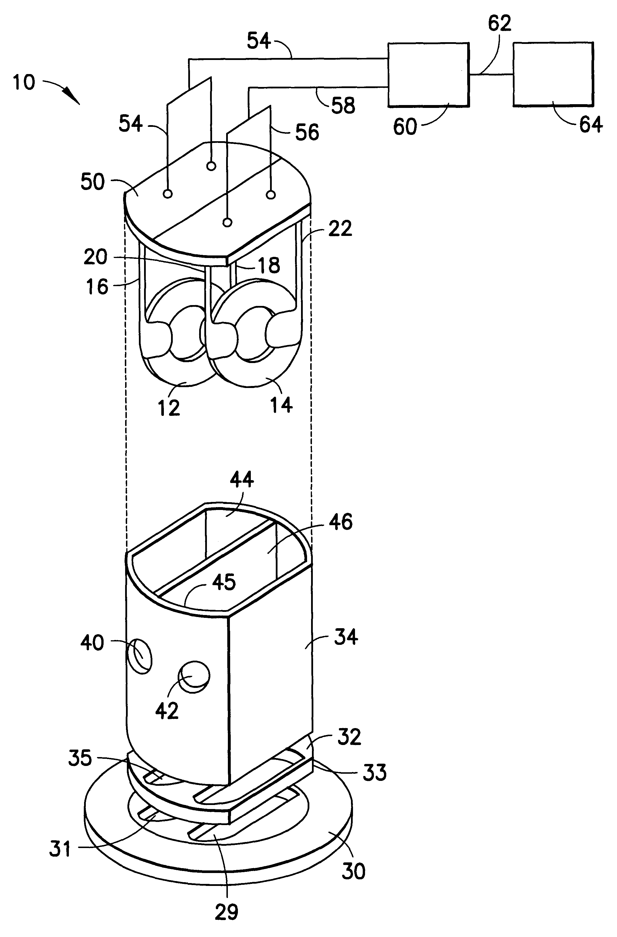
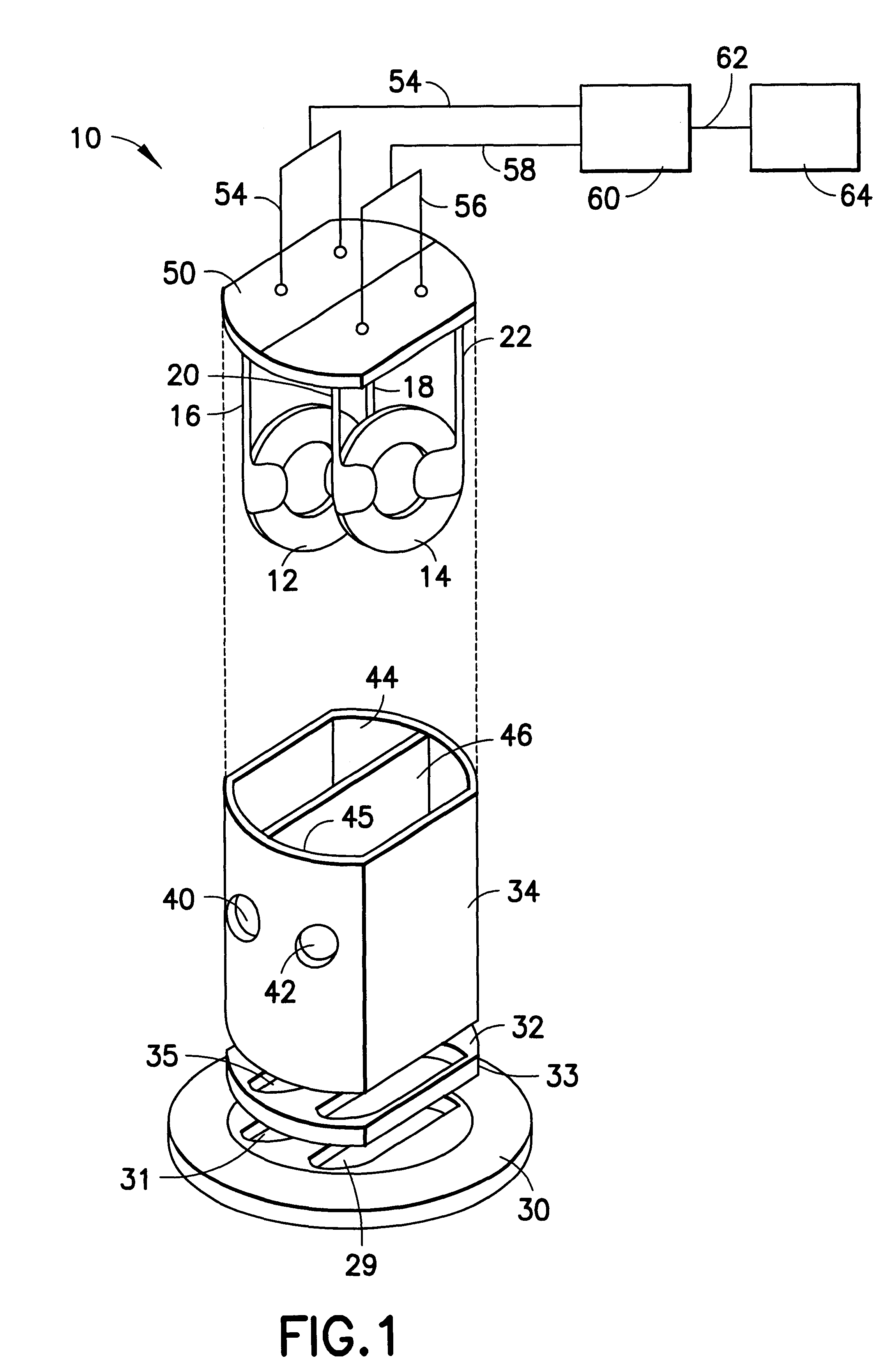
The QMB sensors employed in the practice of the invention utilize a quartz crystal having coated on the surface thereof a coating of sensor material. The sensor material has a sorptive affinity for the gas component(s) of interest, and may for example be selected to be specifically physically adsorptive for a single component of a multi-component gas mixture, e.g., in a gas stream flowed in contact with the QMB sensor.

In operation, an electrical oscillation is imposed on the QMB sensor to produce a frequency response that will vary from the fundamental frequency of the QMB sensor (the fundamental frequency being the frequency response that is gene...


PUM


Abstract

A sensor device for detecting the presence of a gas species in a gas environment susceptible to the presence of same. The sensor device may include a piezoelectric crystal coated with a sensor material having adsorptive affinity for the gas species, with an electric oscillator arranged for applying an oscillating electric field to the piezoelectric crystal to generate an output frequency therefrom indicative of the presence of the gas species when present in the gas environment, when the gas environment is exposed to the piezoelectric crystal. Another aspect of the invention involves a porous polymeric material that may be employed as a sensor material on a piezoelectric crystal sensor device, as well as a quartz microbalance holder that enables reactor gas monitoring. The sensor device alternatively may comprise an optical sensor arranged in a non-contaminating fashion in relation to the gas environment being monitored.

Description

1. Field of the InventionThe present invention generally relates to sensors for detecting gaseous components in gaseous environments containing same, to novel sensing materials useful in such sensors, and to semiconductor manufacturing process systems comprising such sensors.2. Description of the Related ArtIn the field of semiconductor manufacturing, wafer substrates are processed in reactor vessels in a variety of unit operations, such as deposition of thin film materials, e.g., by metalorganic chemical vapor deposition (MOCVD), etching (of the wafer and / or microelectronic device structures fabricated thereon), plasma treatment, ion implantation, etc. In addition, the reactor vessel itself may be subjected to cleaning by operations such as chamber etching, solvent flow-through, and elevated temperature volatilization of deposits.The aforementioned operational functions are typically conducted for a given amount of time, as opposed to determining an endpoint for the process step by...

Claims


Application Information

Patent Timeline
IPC IPC(8): B01D53/02G01N29/02G01N27/00G01N29/22G01N29/32G01N29/036G01N33/00
CPCB01D53/02G01N29/036G01N29/323G01N29/326G01N2033/0095
Inventor TOM, GLENN M.KING, MACKENZIE E.
Owner LIFE SAFETY GERMANY
Why Eureka
Try Eureka