Method and apparatus for circuit designing of an LSI circuit without error paths

a circuit design and circuit technology, applied in the direction of cad circuit design, program control, instruments, etc., can solve the problems of error paths, lsi circuit size and complexity, and wiring has not yet been decided among the cells,

Inactive Publication Date: 2001-10-23
FUJITSU LTD
View PDF3 Cites 20 Cited by
  • Summary
  • Abstract
  • Description
  • Claims
  • Application Information

AI Technical Summary

Problems solved by technology

At this time, however, wiring has not beer decided yet among the cells.
With an advance in a micro fabrication art in recent years, a LSI has become extremely large in its circuit size and complex.
Therefore, simple arranging of the cells or wiring among the cells without any indices is liable to lead to the occurrence of error paths.
However, even if the critical path is recognized at this time, it is difficult to cancel this critical path during rearranging or rewiring, and thus logical designing must be performed again.
Furthermore, dur

Method used


Image

  • Method and apparatus for circuit designing of an LSI circuit without error paths
  • Method and apparatus for circuit designing of an LSI circuit without error paths
  • Method and apparatus for circuit designing of an LSI circuit without error paths

Examples


Embodiment Construction

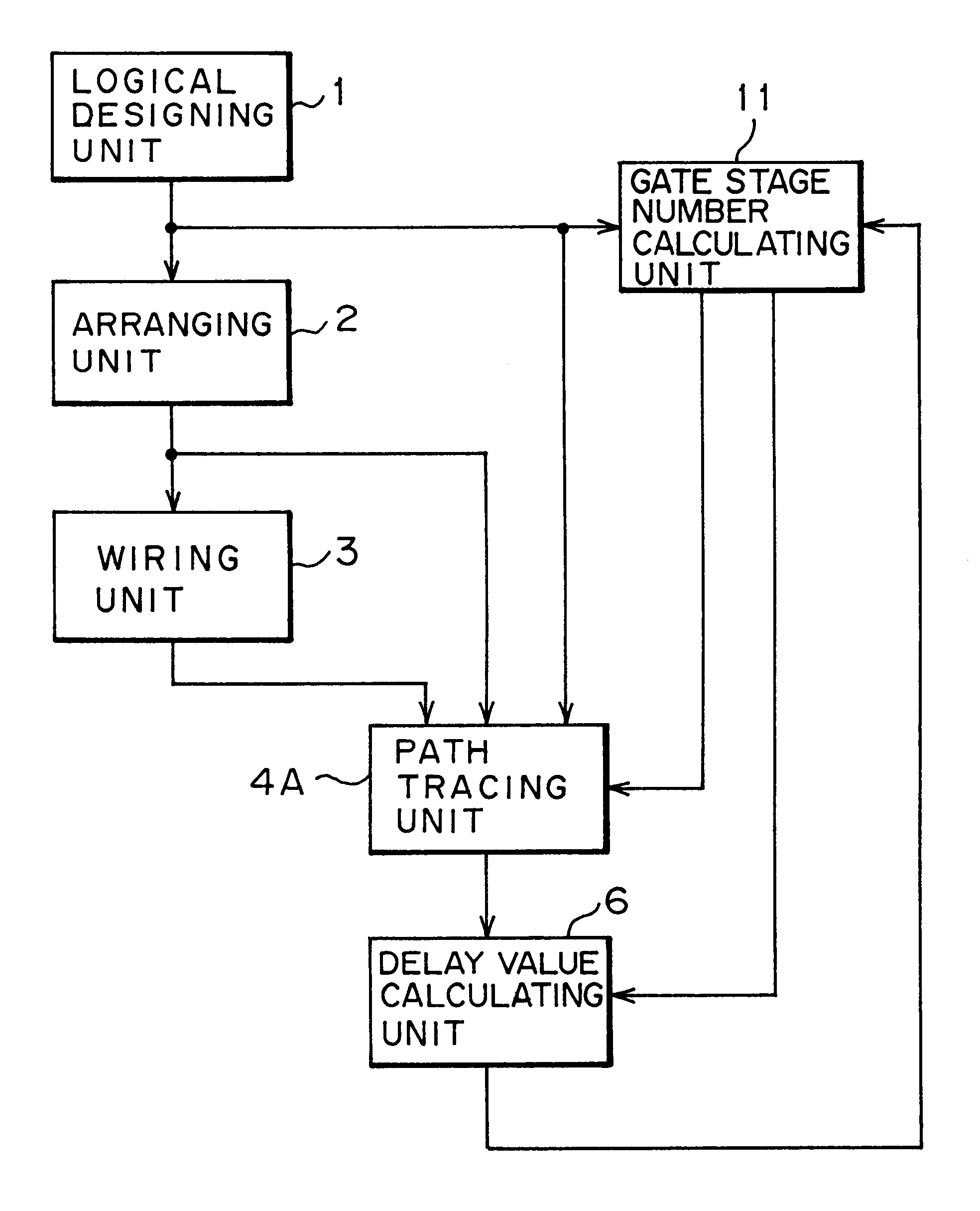
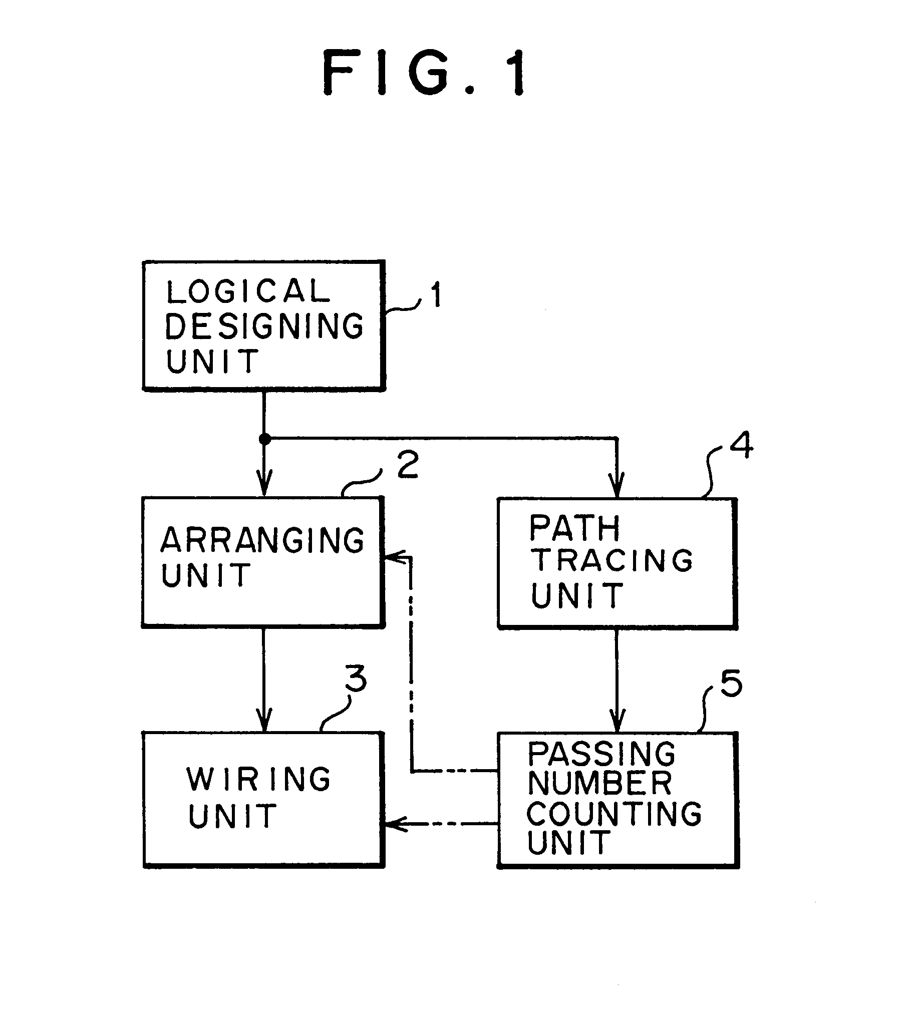
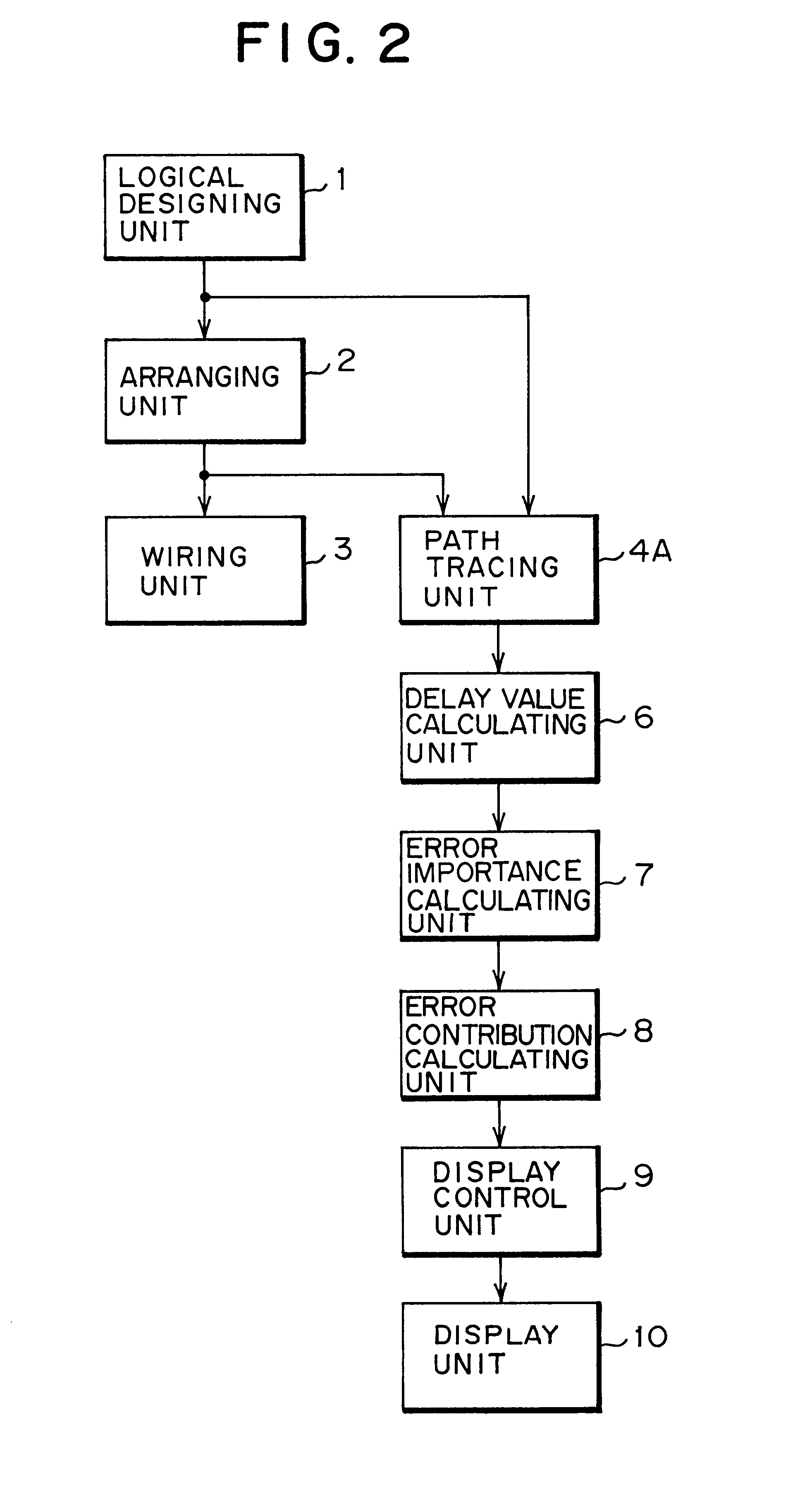
The preferred embodiments of the present invention will be described below with reference to the accompanying drawings.

Referring first to FIG. 6 which is a block diagram, there is shown a functional construction of a circuit designing apparatus of an embodiment of the present invention. As shown in the drawing, a processor 20 provided with a display (display unit) 21, an input unit 22, a keyboard 22a and a mouse 22b functions as the circuit designing apparatus of the embodiment.

The display 21 displays information necessary for circuit designing performed by the processor 20 and the progress of its circuit designing. The keyboard 22a and the mouse 22b are operated by a designer (operator) and used for inputting various bits of information regarding circuit designing. Accordingly, the designer can perform circuit designing (including logical designing, arranging and wiring) in an interactive manner by inputting various bits of information through the keyboard 22a and the mouse 22b whi...


PUM


Abstract

There are disclosed a method and an apparatus for circuit designing, which enable arranging and wiring operations to be efficiently performed by using indices for arranging and wiring without the occurrence of any error paths. In the method and apparatus for circuit designing, path tracing is performed from one or more tracing start pins for a result of logical designing and the number of passing through each pin of cells to be arranged is counted during the path tracing. Thus, the method and apparatus for circuit designing are suitably used for designing of a circuit such as a LSI or the like, which has been enlarged in size and complex following an advance in a micro fabrication art.

Description

1) Field of the InventionThe present invention relates to a method and an apparatus suitably used for circuit designing of a LSI, which has become larger in its size and more complex following an advance in a micro fabrication art in recent years.2) Description of the Related ArtGenerally, LSI designing is performed based on a procedure shown in FIG. 14. This procedure includes steps as follows. First, logical designing is performed for a circuit (LSI) to be designed (step S1), then cells (circuit elements) are arranged based on the result of this logical designing (step S2) and a timing is checked for the result of this arrangement (step S3).For a timing check, a delay value is calculated for each path while performing path tracing for the arranging result of the cells, and determination is made as to whether this value satisfies a timing condition or not. At this time, however, wiring has not beer decided yet among the cells. Thus, a delay value for each path is calculated by esti...

Claims


Application Information

Patent Timeline
IPC IPC(8): G06F17/50H01L21/82
CPCG06F17/5031G06F17/5068G06F30/3312G06F30/39
Inventor SUGIYAMA, HIROYUKIABE, YASUNORIBIZEN, NAOMI
Owner FUJITSU LTD
Why Eureka
Try Eureka