
Error catch RAM for memory tester has SDRAM memory sets configurable for size and speed

a memory tester and error catch technology, applied in the direction of memory adresing/allocation/relocation, instruments, digital storage, etc., can solve the problem of not preserving the rated speed operation for random addressing, slow performance, and inability to support the same abilities or modes of operation

Inactive Publication Date: 2001-11-20
VERIGY PTE
View PDF1 Cites 45 Cited by
  • Summary
  • Abstract
  • Description
  • Claims
  • Application Information

AI Technical Summary

Problems solved by technology

Lack of locality is not fatal, but if consistently violated the result is doggy slow performance.
Works with R100 (12 Banks), R33 (4 Banks) and L100 (1 Bank), but does not preserve rated speed operation for Random addressing.
This does not mean, however, that these same abilities or modes of operation cannot be supported by the SRAM Memory Sets.
Experience suggests that the above memory mode / configuration and transaction information can require a significant amount of time to digest.
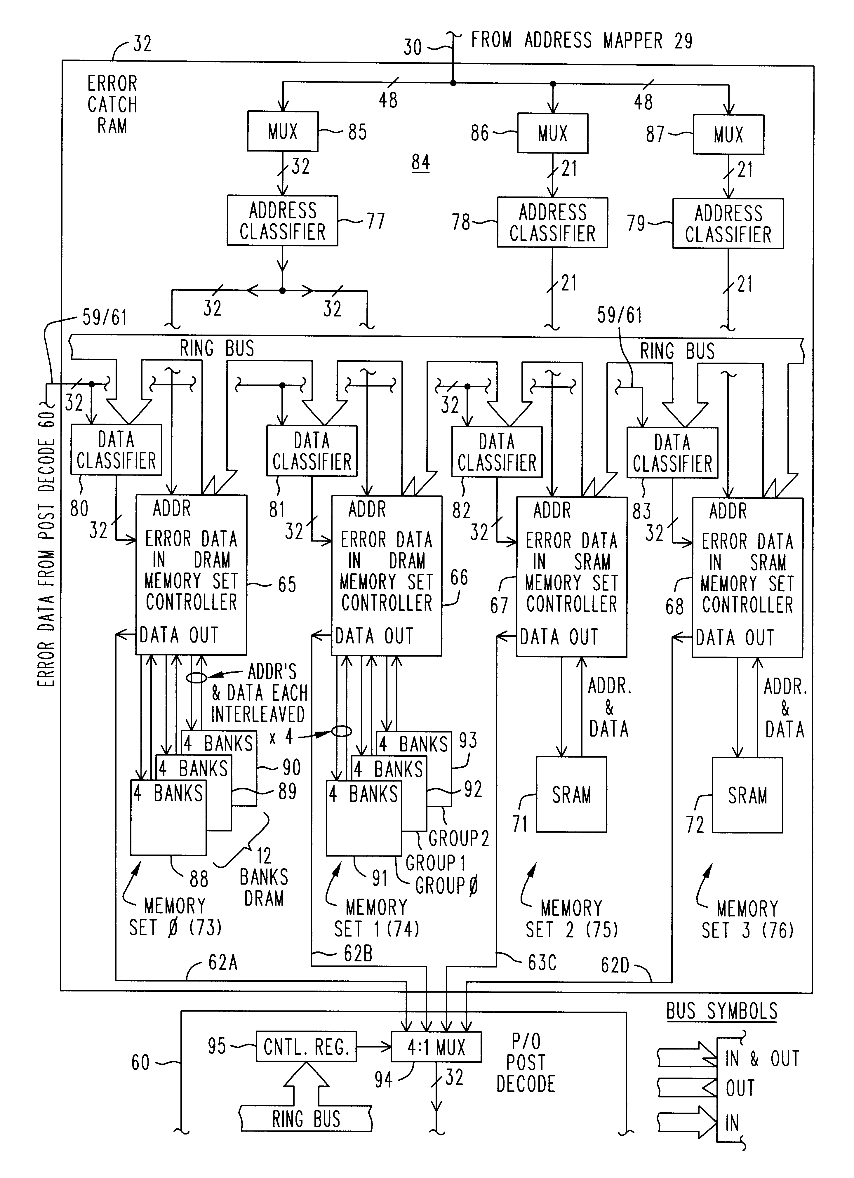
Now, cases (A) and (B) can not safely be assumed to always be write operations, even though it is readily appreciated that for R100 and R33 operation, there is no guarantee whatsoever that a read operation to an address will produce the last data that was written to that address.
Composing across Groups in R33 would be like adding account numbers for different credit cards; the result is not a useful account number!
Those twelve clock cycles do not, however, get the composed data stored anywhere.
Secondly, FCP is fast because it does both the read and the write using only one instance of addressing for each location in a Bank.
A write operation to that region of memory will potentially (probably will) ruin the composition at the address written to, and is used to clear the flag.
Any OLW done in the Memory Set (OLW_MS#N 195) is a potential threat to the integrity of the composed results, and is used to clear the flag.

Method used


Image

  • Error catch RAM for memory tester has SDRAM memory sets configurable for size and speed
  • Error catch RAM for memory tester has SDRAM memory sets configurable for size and speed
  • Error catch RAM for memory tester has SDRAM memory sets configurable for size and speed

Examples


Embodiment Construction

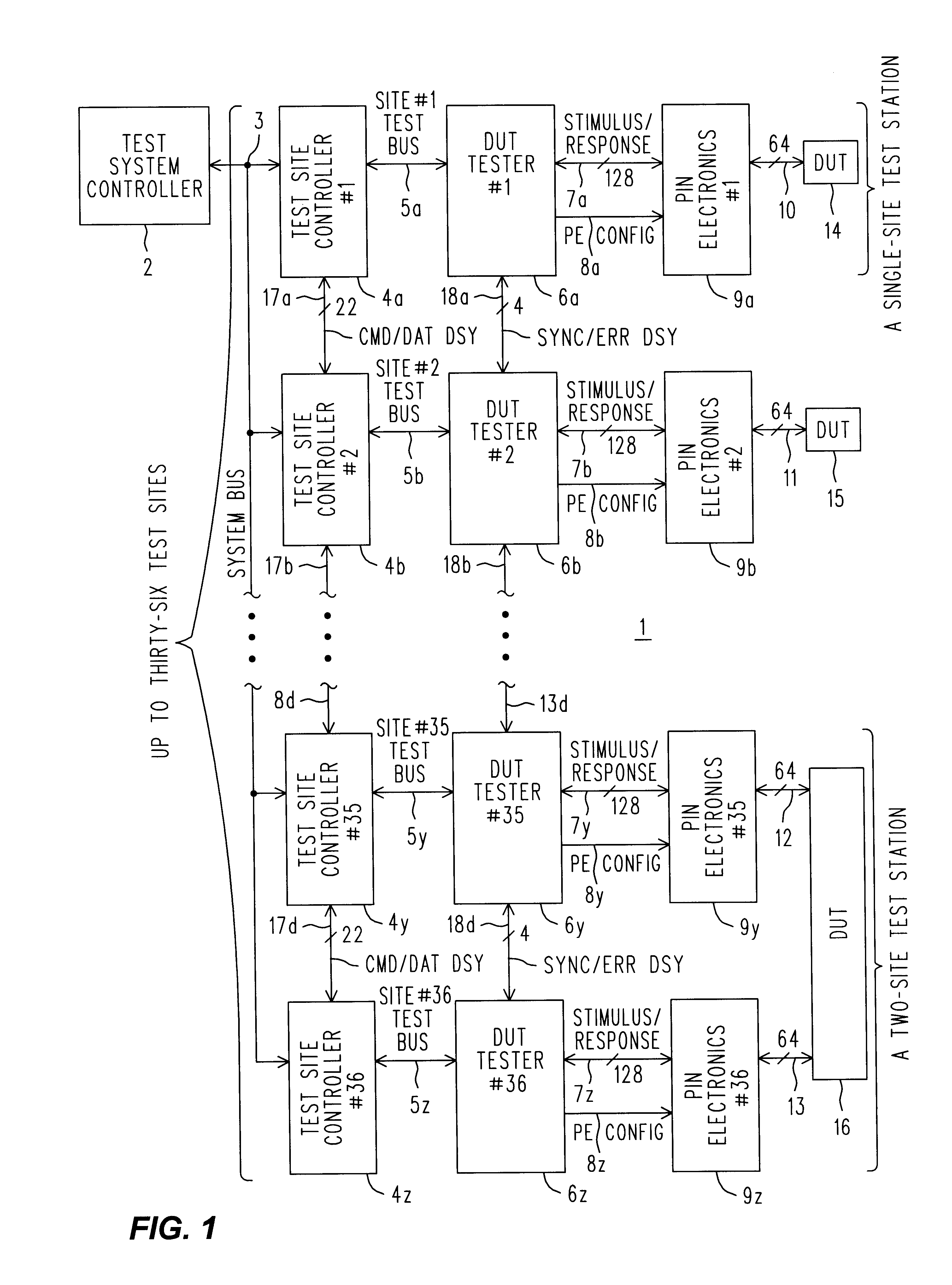
Refer now to FIG. 1, wherein is shown a simplified block diagram 1 of a Non-Volatile Memory Test System constructed in accordance with the principles of the invention. In particular, the system shown can simultaneously test, with as many as sixty-four test points each, up to thirty-six individual DUT's (Devices Under Test) at one time, with provisions for reconfiguration to allow elements of a collection of test resources to be bonded together to test DUT's having more than sixty-four test points. These test points may be locations on a portion of an integrated circuit wafer that has not yet been diced and packaged, or they might be the pins of a packaged part. The term "test point" refers to an electrical location where a signal may be applied (e.g., power supplies, clocks, data inputs) or where a signal can be measured (e.g., a data output). We shall follow the industry custom of referring to the test points as "channels". The "collection of test resources to be bonded together" r...


PUM


Abstract

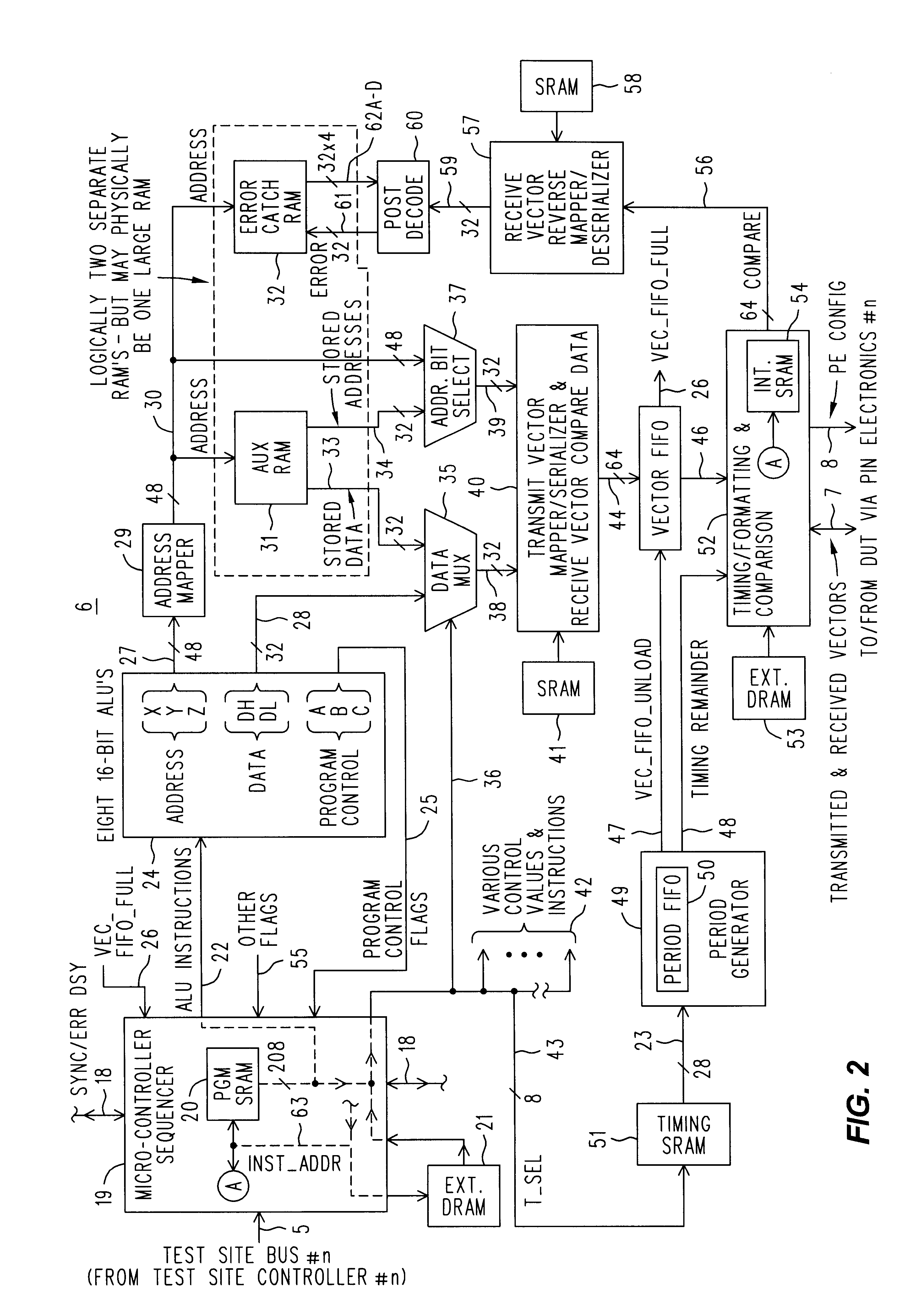
DRAM speed of operation in an Error Catch RAM can be increased by a combination of interleaving signals for different Banks of memory in a Group thereof and multiplexing between those Groups of Banks. A three-way multiplexing between three Groups of four Banks each, combined with a flexible four-fold interleaving scheme for signals to a Group produces an increase in speed approaching a factor of twelve, while requiring only three memory busses. Each of the twelve Banks represents the entire available address space, and any individual write cycle might access any one of the twelve Banks. A utility mechanism composes results for all twelve Banks during a read cycle at an address into a unified result. There is a mechanism to track of the integrity of the composed results, as further write operations can produce the need for another composing step. There are four Memory Sets, two are "internal" SRAM's and two are "external" DRAM's. The SRAM's are integral parts of VLSI circuits, while the DRAM's are individual packaged parts adjacent that VLSI. The amount of DRAM is optional. For DRAM memory sets the multiplexing and interleaving mode allows full random access at speeds of up to 100 MHz. For speeds will not exceed 33 MHz, the DRAM's can be configured to provide three times the depth in return for the lower speed by removing the multiplexing between Groups in favor of just interleaving upon one larger Group; Bank enable bits that were used as part of the multiplexing can now be used as regular address bits to increase the size of the address space of the one Group that remains. If the testing to the DUT fits the "linear" mode of access, a twelve-fold increase in memory depth is available, even when the DUT is tested at the highest speed the tester can operate at. This eliminates the interleaving scheme in favor of addressing within a single Bank at a time. Another reconfiguration is to combine the external memory sets into one memory set that has twice the depth of either uncombined set, regardless of other (i.e., the speed related) modes of operation.

Description

Electronics devices and capabilities have grown extremely common in daily life. Along with personal computers in the home, many individuals carry more than one productivity tool for various and sundry purposes. Most personal productivity electronic devices include some form of non-volatile memory. Cell phones utilize non-volatile memory in order to store and retain user programmed phone numbers and configurations when the power is turned off. PCMCIA cards utilize non-volatile memory to store and retain information even when the card is removed from its slot in the computer. Many other common electronic devices also benefit from the long-term storage capability of non-volatile memory in un-powered assemblies.Non-volatile memory manufacturers that sell to the electronic equipment manufacturers require testers to exercise and verify the proper operation of the memories that they produce. Due to the volume of non-volatile memories that are manufactured and sold at consistently low price...

Claims


Application Information

Patent Timeline
Patent Type & Authority Patents(United States)
IPC IPC(8): G11C29/56G06F12/06G01R31/28G06F12/16G11C7/00
CPCG11C29/56G11C7/00
Inventor COOK, III, JOHN H.SINGH, PREET P.DE LA PUENTE, EDMUNDO
Owner VERIGY PTE
Learn More