
Semiconductor device manufacturing method

Inactive Publication Date: 2001-12-04
FUJITSU LTD
View PDF9 Cites 68 Cited by
  • Summary
  • Abstract
  • Description
  • Claims
  • Application Information

AI Technical Summary

Problems solved by technology

In recent years, with the progress of miniaturization in the semiconductor device, it has become difficult to isolate devices with good precision by using the device isolation method which employs the LOCOS (Local Oxidation of Silicon) method employed in the prior art.
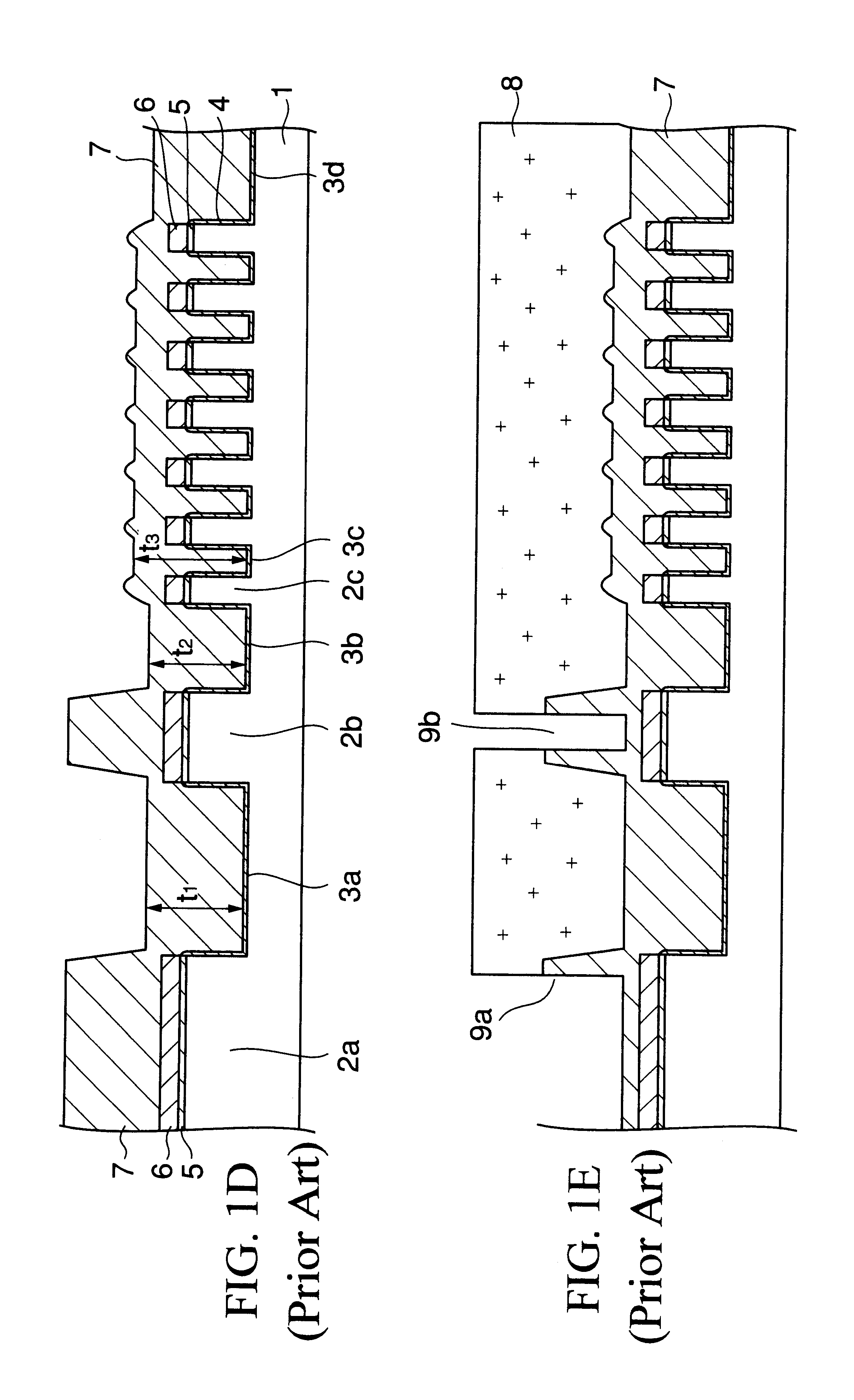
Hence, according to the above method, variation of the film thickness of the silicon oxide film 7 cannot be overcome.
On the contrary, according to the prior art, i.e., if the polishing is executed without the first step polishing only under the same conditions as those for the second step polishing, it becomes impossible to control the polishing of the fine convex regions because the polishing is affected by the density of the patterns on the polished substrate.
This is because such pressure slightly affects the polishing rate.

Method used


Image

  • Semiconductor device manufacturing method
  • Semiconductor device manufacturing method
  • Semiconductor device manufacturing method

Examples


second example

In the condition shown in FIG. 7D, MIRRA-3400 (product name) manufactured by Applied Material Co., Ltd. is employed as the polishing equipment used to polish the silicon oxide film 27, and then the first step polishing and the second step polishing are carried out.

In the second example, the abrasive cloth and the slurry which are the same as those in the first example are employed.

The conditions for the first step polishing are given in Table 4, and also the conditions for the second step polishing are set forth in Table 5.

TABLE 5

In the first step polishing step, like the first example, the silicon oxide film 27 which is projected on the third device region 22c having the narrow area is ready to be physically removed due to contact of the hard abrasive cloth 102. On the contrary, since the silicon oxide film 27 on the first device region 22a having the wide area is mechanically strong and also the slurry is difficult to react chemically with the silicon oxide film 27 as the polishin...

third example

In the condition shown in FIG. 7D, MIRRA-3400 (product name) manufactured by Applied Material Co., Ltd. is employed as the polishing equipment used to polish the silicon oxide film 27, and then the first step polishing and the second step polishing are carried out.

In the third example, the polishing conditions except the slurry used in the first step polishing are set identically to those in the second example. In the third example, slurry in which SS-25 (product name) containing KOH as the dispersant Is diluted with the ionized water is employed as the slurry used in the first step polishing. In this case, if an amount of SS-25 is assumed to 1, an amount of the ionized water is set to 2.5. Also, slurry which contains silica or cerium oxide (CeO.sub.2) as the abrasive grain contained in the slurry may be employed. Also, slurry which contains NH.sub.4 OH as the dispersant may be employed.

The conditions for the first step polishing are given in Table 6, and also the conditions for the...

second embodiment

It has already been described that, in order to polish the buried insulating film on the active region of the semiconductor wafer in which FRAM cells, SRAM cells, or the like are formed and the scribe line region for splitting the wafer, there is such a possibility that the dishing of the buried oxide film occurs in the trench.

Therefore, TEG patterns 61 shown in FIG. 26 are formed at plural locations of the semiconductor wafer shown in FIG. 25, and then occurring situation of the dishing of the buried oxide film on the trench is checked.

This TEG pattern 61 has a plural of active pattern in which the maximum single active pattern has an area of 800 .mu.m .times.600 .mu.m.

As shown in FIG. 26, in the TEG pattern 61, a square trench 63 having depth of 380 nm is formed in a region, which is surrounded by a scribe line 62 having a width of 100 .mu.m, of the silicon wafer 60. A length L1 of one side of the trench 63 is 20 mm from a center of the scribe line 62. A first active pattern conge...


PUM


Abstract

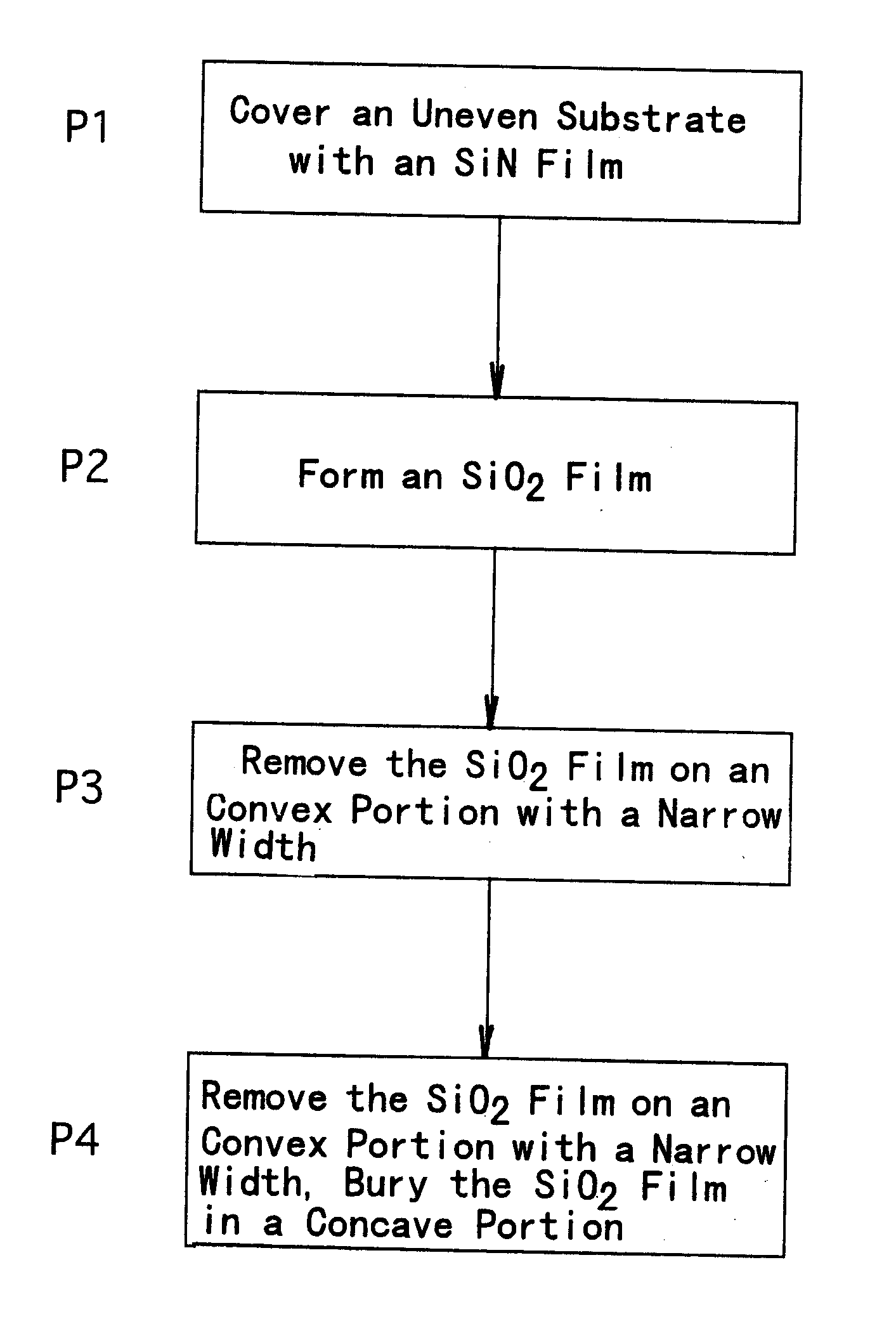
The present invention relates to a semiconductor device manufacturing method containing the step of polishing an insulating oxide film having an uneven surface, to improve a throughput in burying the insulating film into trenches and also improve flatness of a polished surface. The method comprises a step of forming a polishing stopping film 26 on a surface of a semiconductor substrate 21, a step of forming trenches 23a to 23d by etching the semiconductor substrate 21 via the opening portions, a step of forming an insulating film 27 in the trenches 23a to 23d and on the semiconductor substrate 21, and steps of first polishing the insulating film by using a first abrasive cloth 102 which has a polishing surface with first hardness while supplying a first slurry onto a polished surface of the insulating film 27 and then polishing the polished surface of the insulating oxide film 27 by using a second abrasive cloth 101 which has second hardness softer than the first hardness while supplying a second slurry onto the polished surface of the insulating film 27 until the polishing stopping film 26 is exposed.

Description

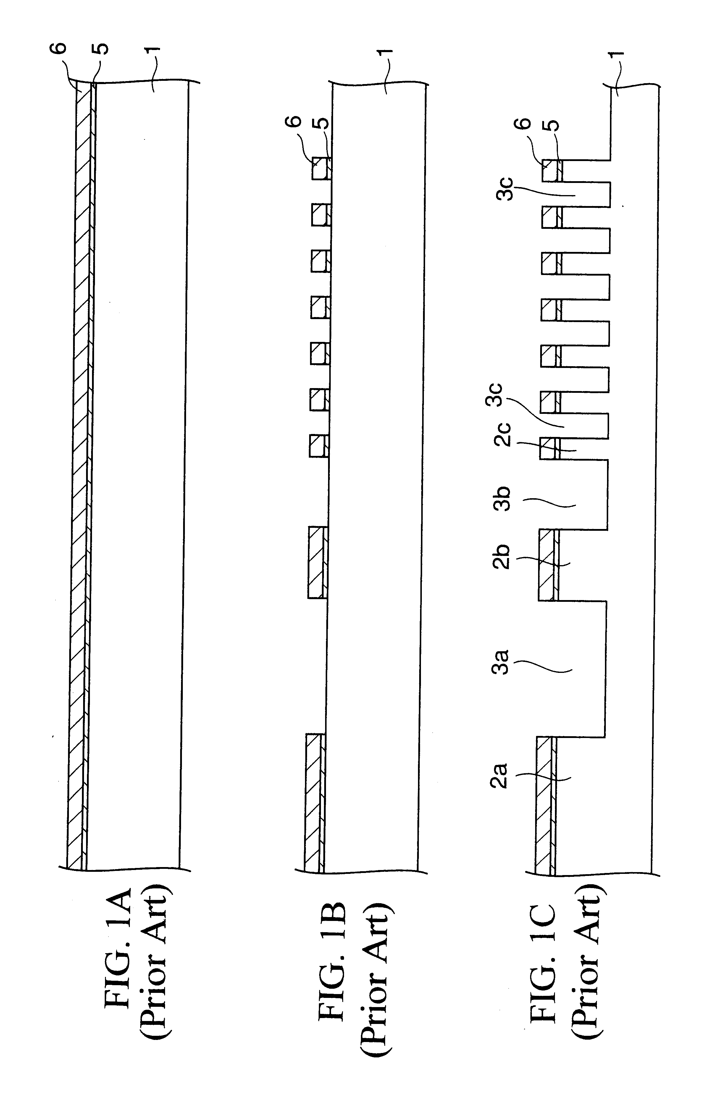
1. Field of the InventionThe present invention relates to a semiconductor device manufacturing method and, more particularly. a semiconductor device manufacturing method including the step of forming a shallow trench isolation (STI).2. Description of the Prior ArtIn recent years, with the progress of miniaturization in the semiconductor device, it has become difficult to isolate devices with good precision by using the device isolation method which employs the LOCOS (Local Oxidation of Silicon) method employed in the prior art.For this reason, the method using the shallow trench has engaged public attention as the new device isolation method in place of the LOCOS method, and has already been utilized.FIGS. 1A to 1G are sectional views showing steps of forming shallow trenches in the prior art.First, as shown in FIG. 1A, an oxide film 5 and a nitride film 6 are formed on a surface of a silicon substrate 1 in this sequence.Then, as shown in FIG. 1B, the oxide film 5 and the nitride fi...

Claims


Application Information

Patent Timeline
IPC IPC(8): B24B37/04B24B49/12B24B49/04B24B49/02H01L21/762H01L21/70H01L21/02H01L21/3105H01L23/544H01L21/304
CPCB24B37/013B24B37/042B24B37/24B24B37/26B24B49/04B24B49/12H01L21/31053H01L21/76229H01L23/544H01L2223/54426H01L2223/54453H01L2924/0002H01L2924/00H01L21/304
Inventor HATANAKA, MASANOBUTAKADA, NAOYUKIMIYAJIMA, MOTOSHUMIYATA, SHUICHI
Owner FUJITSU LTD
Features
  • Generate Ideas
  • Intellectual Property
  • Life Sciences
  • Materials
  • Tech Scout
  • Unparalleled Data Quality
  • Higher Quality Content
  • 60% Fewer Hallucinations
Learn More