Process, voltage, temperature independent switched delay compensation scheme

a delay compensation and temperature independent technology, applied in the field of digital delay locked loops, can solve the problems of inability to predict the amount of jitter between 200 ps and 300 ps, and the inability to detect the phase differen

Inactive Publication Date: 2001-12-04
CONVERSANT INTPROP MANAGEMENT INC
View PDF6 Cites 115 Cited by
  • Summary
  • Abstract
  • Description
  • Claims
  • Application Information

AI Technical Summary

Problems solved by technology

In order to hold the locked condition, the delay line is continuously increased and decreased in step increments around a lock point, which results in inherent tracking jitter.
However, with the advent of tighter access time (T.sub.ac) specifications for double data rate (DDR) SDRAMs which are synchronized to the rising and falling edges of a system clock rather than only to the rising edge, even an amount of jitter of 200 ps-300 ps is becoming intolerable, considering the numerous sources adding to this jitter apart from the DDL, including input clock to data skew, clock duty cycle variations, inaccuracies in the actual input and output buffer delays with respect to its design model, etc.
This mismatch is highly dependent on the manufacturing process, and thus is hard to predict in the design stage.
As the operating frequencies continue to increase, the switching jitter can undesirably reduce the data eye significantly.
In addition, since this switching occurs only infrequently, it is inherently hard to detect during testing and can cause apparently randomly dropped bits when the part is in use in the field.
However, most analog based DLL designs employ some form of charge pumps for voltage controlled delay lines and as such they suffer from a limited resolution of the delay steps since the controlling element affects an entire delay line.
In addition such DLLs often require a large acquisition time due to loop bandwidths being limited to a small fraction of the clock frequency to ensure stability of the loop.
This effect also causes a poor jitter performance in analog DLLs.
Furthermore, analog DLL designs are inherently more susceptible to all sources of noise as their control variables (usually voltage) are reduced to achieve finer resolutions.
In particular, SDRAMs provide a very noisy environment for analog blocks in form of supply and substrate noise, which when combined with area restrictions in SDRAMs, sometimes preventing adequate implementation of noise prevention techniques through layout, can result in unreliable DLLs in noisy field environments.

Method used


Image

  • Process, voltage, temperature independent switched delay compensation scheme
  • Process, voltage, temperature independent switched delay compensation scheme
  • Process, voltage, temperature independent switched delay compensation scheme

Examples


Embodiment Construction

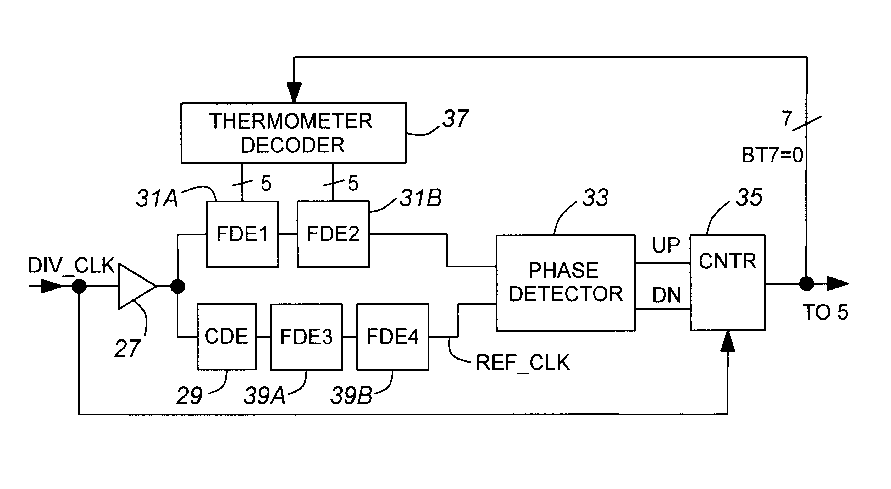
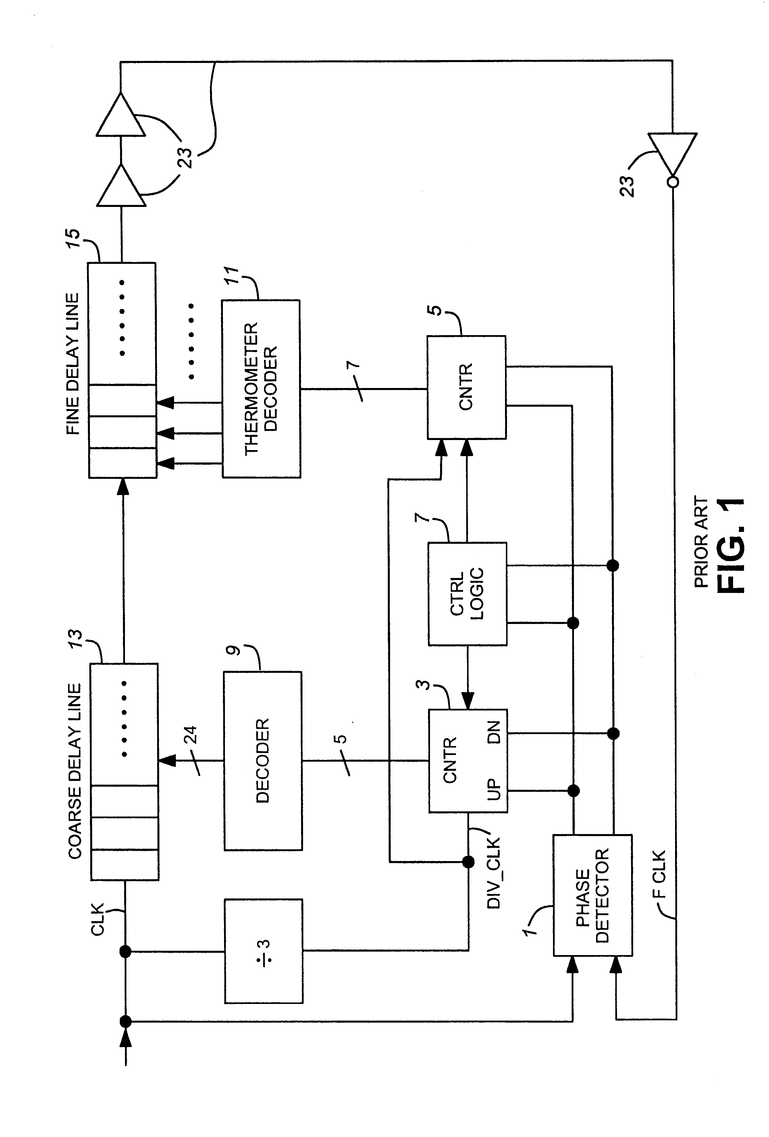
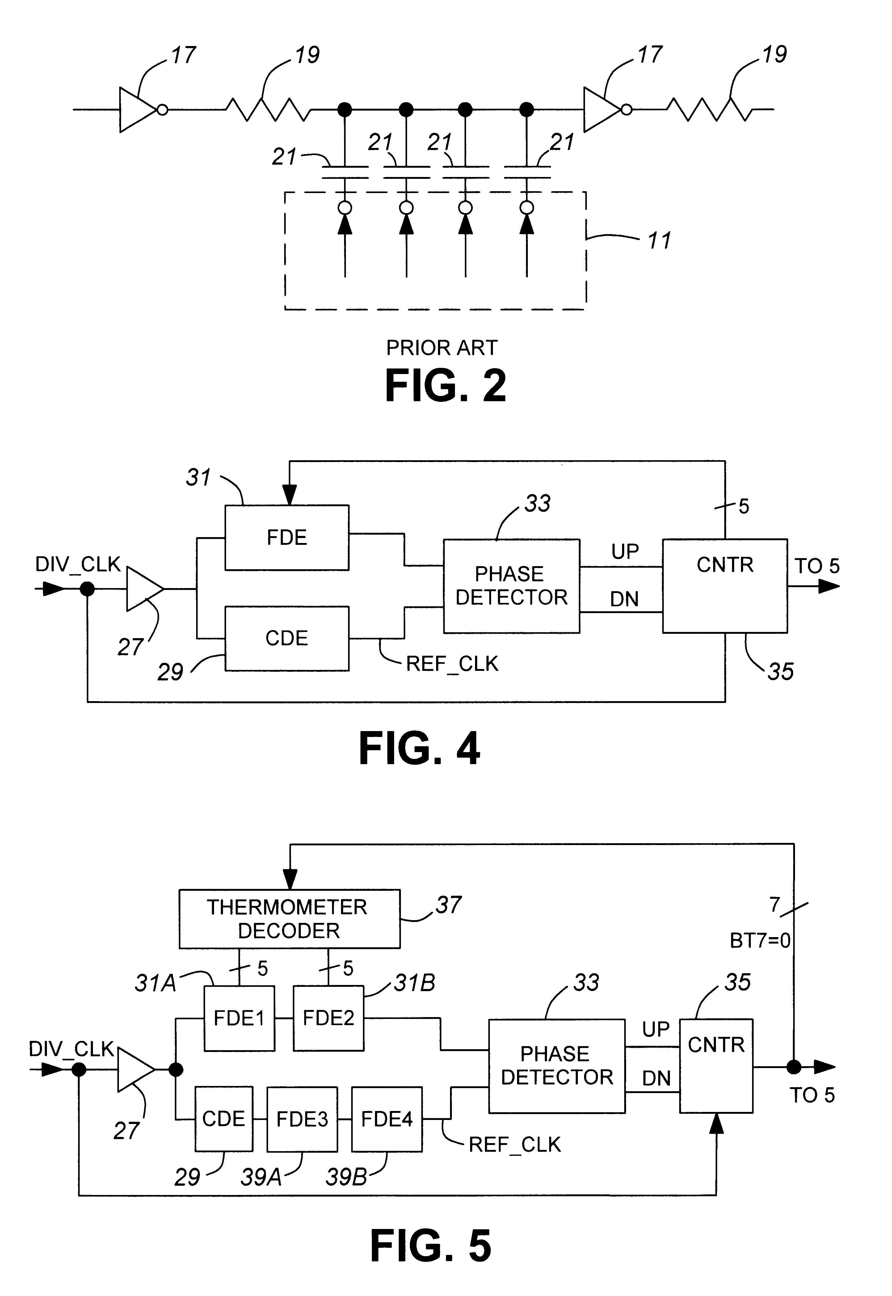
FIG. 1 illustrates a DLL in accordance with the prior art. A phase detector 1 receives a system clock (CLK) signal and a feedback clock (FCLK) signal, compares the phase of the FCLK signal with that of the CLK signal, and issues up and down count control signals to a coarse adjust counter 3, and fine adjust counter 5. The up and down signals are also monitored by a control logic (CTRL LOGIC) circuit 7, which controls counters 3 and 5.

The outputs of the counters 3 and 5 are coupled to decoders 9 and 11, which decode the counter outputs and apply control signals respectively to coarse delay line 13 and to fine delay line 15. The CLK signal is coupled to an input of the course delay line, and the output of the coarse delay line is coupled to the input of the fine delay line. Typically the coarse delay line 13 is formed of RC (resistor-capacitor) delay elements and inverters which are selectively connected in series with each other by respective multiplexers. Preferably the fine delay l...


PUM


Abstract

A delay compensation circuit for a delay locked loop which includes a main delay line having a fine delay line comprising fine delay elements and a coarse delay line comprising coarse delay elements, the main delay line being controlled by a controller, the delay compensation circuit comprising: an adjustable fine delay for modeling a coarse delay element, a counter for controlling the adjustable fine delay to a value which is substantially the same as that of a coarse delay element, a circuit for applying a representation of the system clock to the delay compensation circuit, and a circuit for applying the fine delay count from the counter to the controller for adjusting the fine delay line of the main delay line to a value which is substantially the same as that of a coarse delay element of the main delay line.

Description

This invention relates to circuits in which fine delay elements are swapped with a coarse delay element during tracking, such as in a delay locked loop (DLL), and more particularly to a circuit and method for compensating for tracking differences between switchable coarse and fine delay elements.BACKGROUND TO THE INVENTIONA digital delay locked loop is generally formed of a phase detector which detects the phase difference between a system clock and a feedback clock, and causes adjustment of a time delay circuit in the loop which causes the DLL output clock to be adjusted to lock with the system clock. The time delay is generally formed of an adjustable delay line.Since the delay line is typically adjusted in steps, the finest delay resolution depends on the delay line step increments. In order to hold the locked condition, the delay line is continuously increased and decreased in step increments around a lock point, which results in inherent tracking jitter. In order to decrease th...

Claims


Application Information

Patent Timeline
Patent Type & Authority Patents(United States)
IPC IPC(8): H03L7/08H03L7/081H03L7/089
CPCH03L7/0814H03L7/089H03L7/0818H03L7/06H03L7/093
Inventor BHULLAR, GURPREETALLAN, GRAHAM
Owner CONVERSANT INTPROP MANAGEMENT INC
Why Eureka
Try Eureka