Residue removal by CO2 water rinse in conjunction with post metal etch plasma strip

a technology of etching and residue removal, applied in the field of semiconductor fabrication, can solve the problems of solvent based chemistry exposed shortfalls, chemical erosion, and the potential for unattended erosion of conducting structures, and the effect of not completely eliminating the potential for such unattended erosion

Inactive Publication Date: 2001-12-11
ADVANCED MICRO DEVICES INC
View PDF7 Cites 30 Cited by
  • Summary
  • Abstract
  • Description
  • Claims
  • Application Information

AI Technical Summary

Problems solved by technology

However, more modern processes involving shrinking line width and device designs incorporating misalignments between metal interconnect layers and underlying contact structures have exposed certain shortfalls associated with solvent based chemistry.
The chemical erosion of the metallic interconnect and contact structures is largely the result of the chemical interaction of the residual OH molecules generated by hydroxyl amine solvents, although primary amines can result in a chemical erosion as well.
Although this technique has shown some promise in alleviating some of the chemical and electrochemical processes that can erode the metal interconnect and underlying contact structures, the potential for such unattended erosion of those condu

Method used


Image

  • Residue removal by CO2 water rinse in conjunction with post metal etch plasma strip
  • Residue removal by CO2 water rinse in conjunction with post metal etch plasma strip
  • Residue removal by CO2 water rinse in conjunction with post metal etch plasma strip

Examples


Embodiment Construction

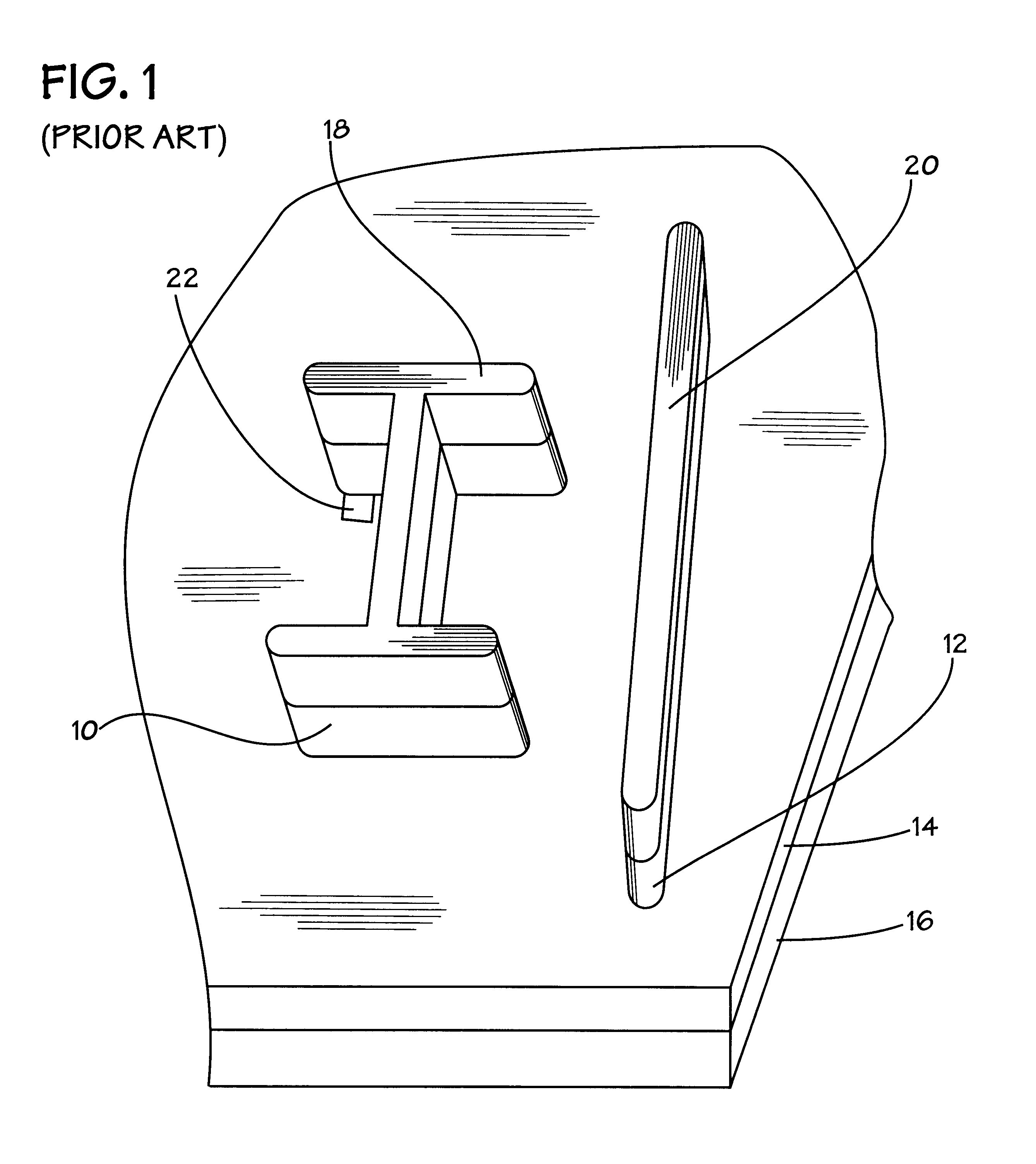
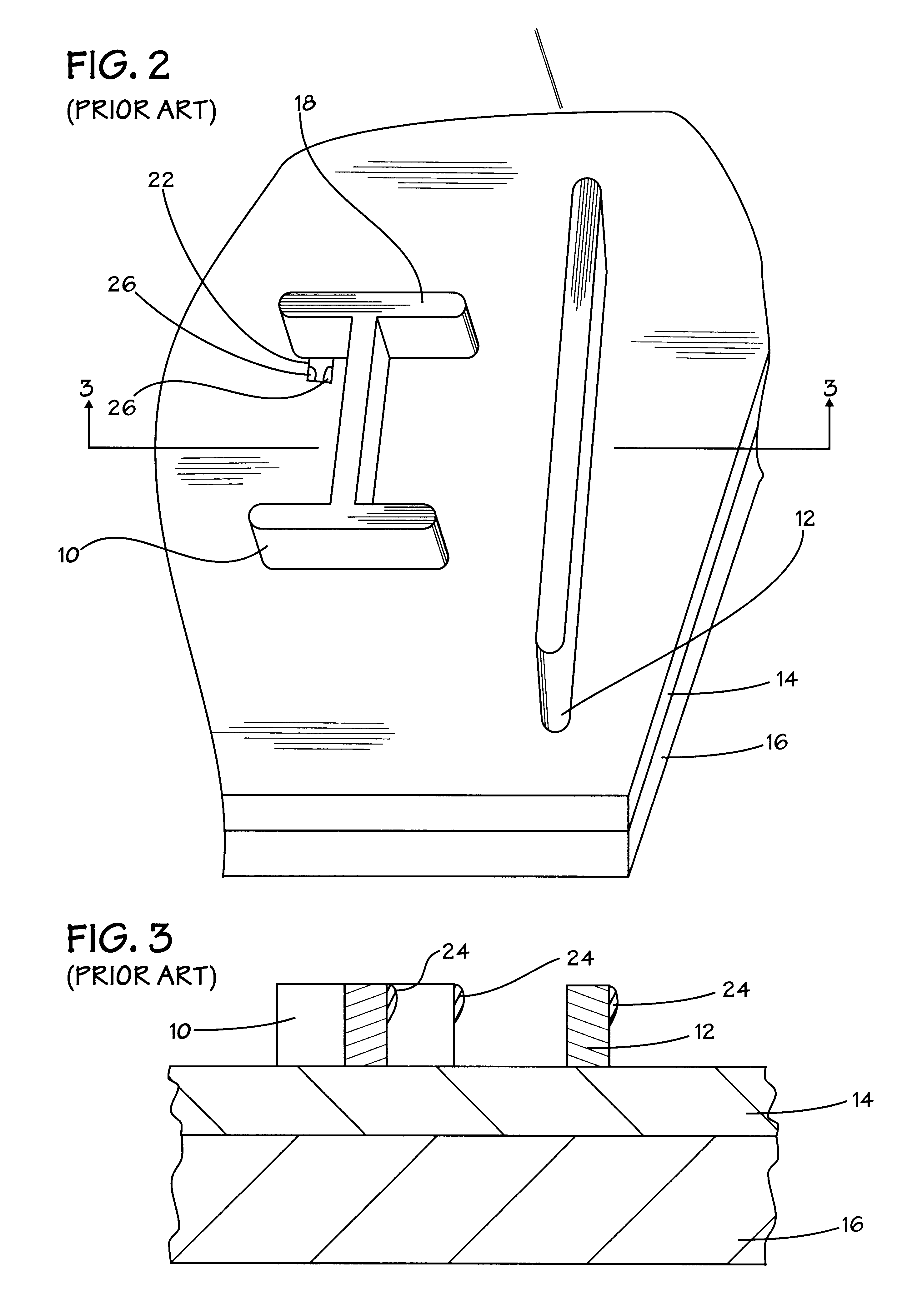
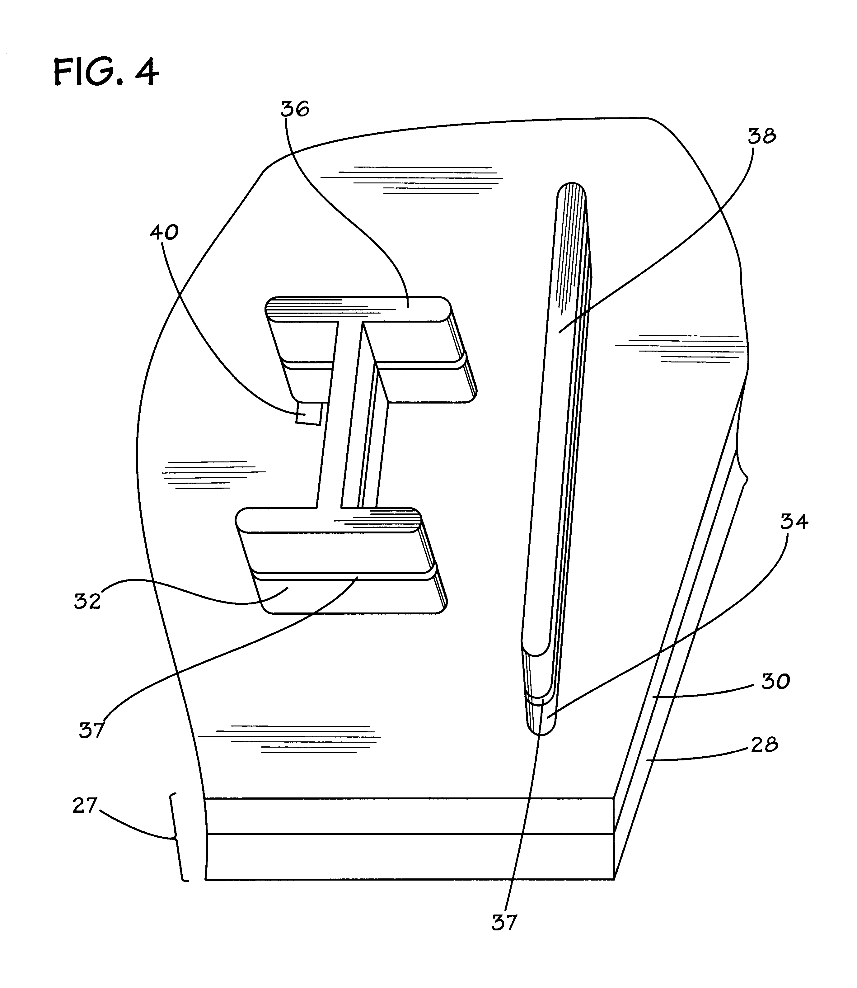
In the drawings described below, reference numerals are generally repeated where identical elements appear in more than one figure. Turning now to the drawings, and in particular to FIGS. 1-3, an exemplary conventional post-metal etch stripping process will be described. FIG. 1 depicts a pictorial view of two metal interconnect structures 10 and 12, which are portions of a larger interconnect layer that is fabricated on an interlevel dielectric layer 14. The interlevel dielectric layer 14 is, in turn, fabricated on a semiconductor substrate 16. FIG. 1 is a depiction of the interconnect structures 10 and 12 just after metal etch but before resist stripping. Accordingly, photomask structures 18 and 20 respectively overlie the interconnect structures 10 and 12. Prior to the etch definition of the interconnect structures 14 and 16, the photomask structures 18 and 20 are patterned into the desired shapes for the interconnect structures 14 and 16. The interconnect structure 10 overlies a ...


PUM

PropertyMeasurementUnit
Flow rateaaaaaaaaaa
Solubility (mass)aaaaaaaaaa
Exposure limitaaaaaaaaaa

Abstract

Methods of removing resist residues from semiconductor workpiece surfaces are provided. In one aspect, a method of removing resist from a surface of a workpiece is provided that includes the steps of exposing the workpiece to a plasma and rinsing the workpiece with CO2 and water in a processing chamber to dissolve the resist. Reliance on post plasma strip solvent rinses for resist removal is eliminated. The combination of CO2 with post-plasma strip water rinse increases the solubility and thus the removal rate of resist residues.

Description

1. Field of the InventionThis invention relates generally to semiconductor fabrication, and more particularly to a method of removing residues from etched metallic surfaces.2. Description of the Related ArtThe fabrication of multi-level metallization structures in integrated circuit processing involves the alternating and sequential fabrication of various metal and interlevel dielectric layers. Interconnections between adjacent metal layers are ordinarily established by means of a plurality of contacts or local interconnects extending through the interlevel dielectric layers that separate the metal layers.The fabrication of metal interconnect layers involves the sequential blanket deposition of metallic material, lithographic resist patterning, and etch to remove the unmasked portions of the deposited metallic layer. Following the etch, the resist is stripped and the remaining surfaces cleansed to remove any residual resist material remaining after the stripping process. Many conven...

Claims


Application Information

Patent Timeline
IPC IPC(8): H01L21/306H01L21/02G03F7/42H01L21/768
CPCG03F7/423H01L21/02054H01L21/02063H01L21/76838
Inventor LEBOWITZ, JOSEPHFAULK, LAURA E.
Owner ADVANCED MICRO DEVICES INC
Why Eureka
Try Eureka