Supercharge Your Innovation With Domain-Expert AI Agents!

Method for integration of integrated circuit devices

a technology of integrated circuits and integrated circuits, applied in the direction of semiconductor devices, electrical equipment, photovoltaic energy generation, etc., can solve the problems of limited success in using epitaxial layers of iii-v materials that do support light emission, and is not economically feasible for two such dissimilar devices

Inactive Publication Date: 2002-01-08
ALTERA CORP
View PDF2 Cites 27 Cited by
  • Summary
  • Abstract
  • Description
  • Claims
  • Application Information

AI Technical Summary

Benefits of technology

It is a further object of this invention to provide such an improved method which allows different devices to be flip-chipped onto a chip or substrate.
It is a further object of this invention to provide such an improved method which allows different devices to be flip-chipped onto a chip or substrate without loss of necessary mechanical support.
It is a further object of this invention to provide such an improved method which allows different photonic devices to be flip-chipped onto a silicon substrate without loss of necessary mechanical support.

Problems solved by technology

The integration of optoelectronic devices with silicon is somewhat problematic for several reasons.
In addition, there has been very limited success in using epitaxial layers of III-V materials that do support light emission, such as gallium arsenide (GaAs) or indium phosphide (InP), in order to grow light emitting structures on silicon substrates because of the lattice mismatch.
It is not economically feasible for two such dissimilar devices to be grown on the same substrate and so it is necessary that separate growth steps be performed for each device type.
Photonic devices that have been integrated onto the surface of a silicon substrate are prone to damage during processing of the wafer unless they are properly protected.
However, when different photonic device types are integrated in separate process steps, repeated application and removal of the underfill has been required.
Removal of epoxy resin is very undesirable as it creates residues that are exceedingly difficult to clean from the substrate surface.

Method used


Image

  • Method for integration of integrated circuit devices
  • Method for integration of integrated circuit devices
  • Method for integration of integrated circuit devices

Examples


Embodiment Construction

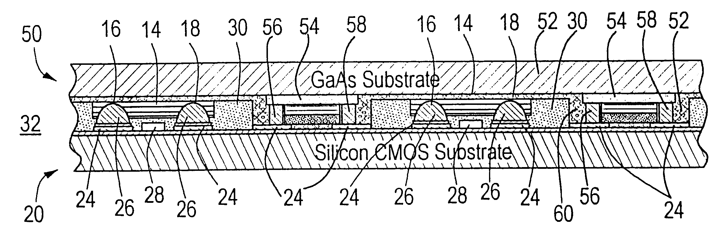
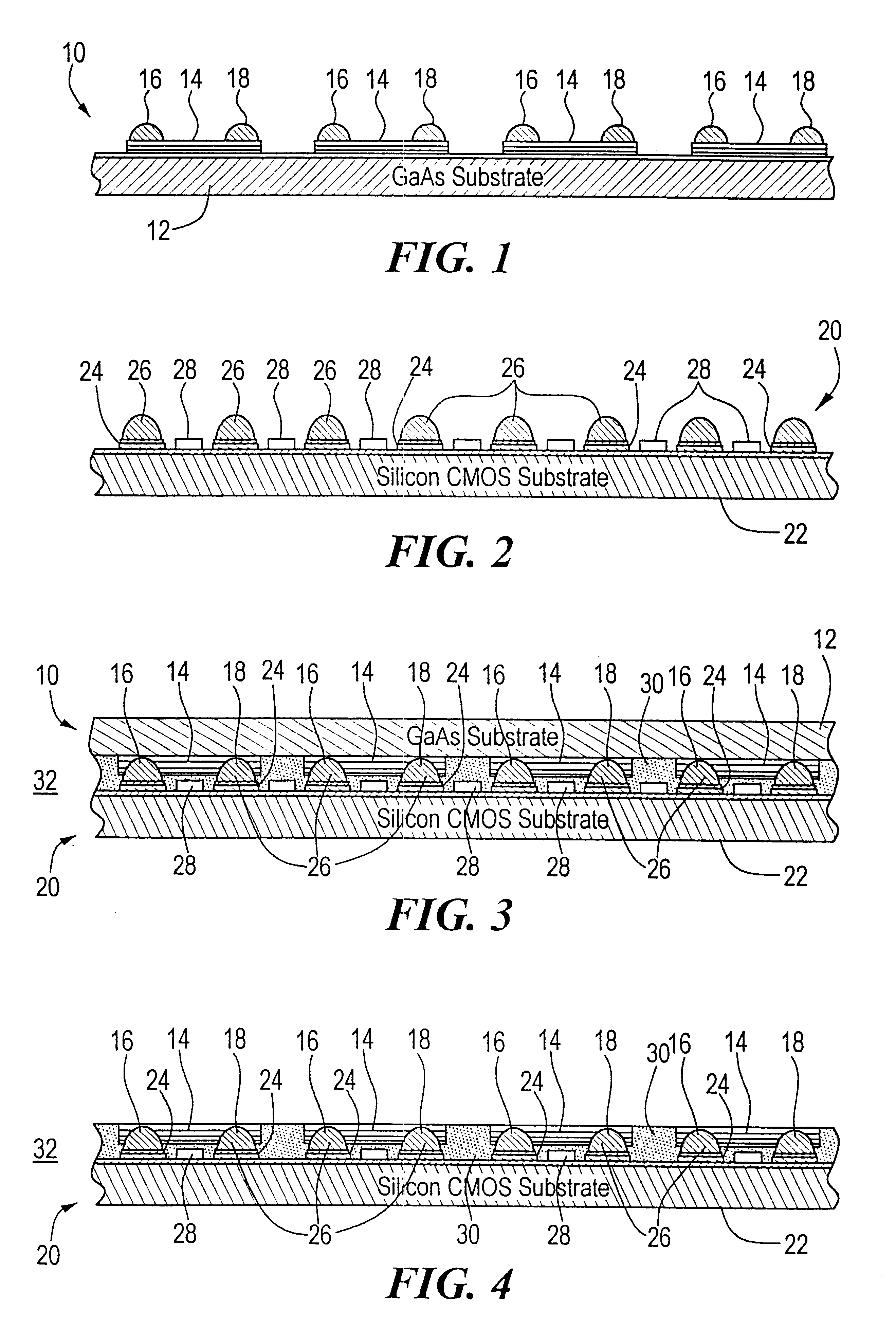
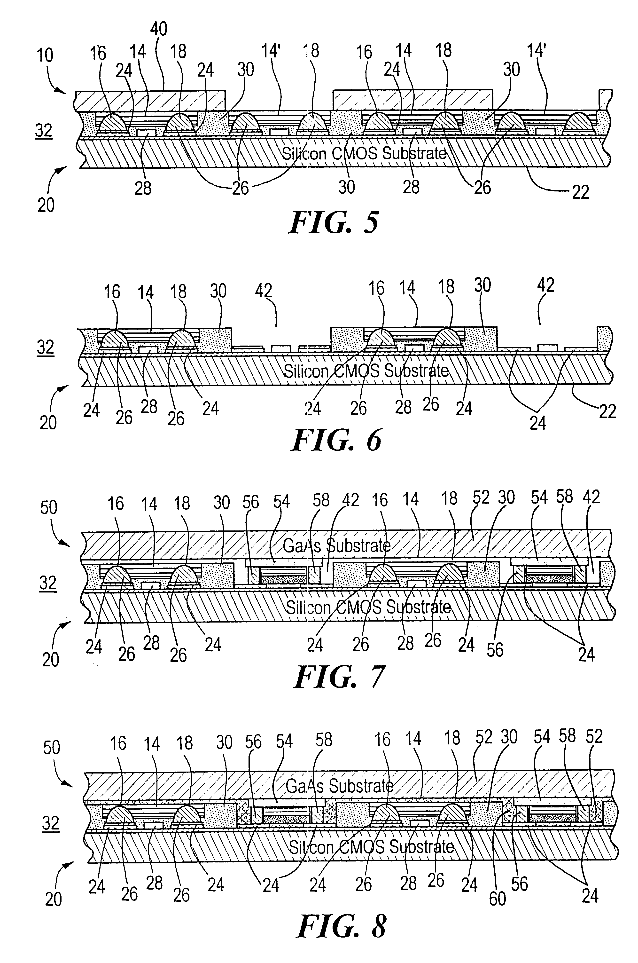
This invention relates to a method of integrating multiple types of devices onto a substrate. In the specific embodiment shown here the devices are photonic devices and they are eventually mounted on a silicon substrate. Specifically the devices are laser emitters and p-i-n detectors and the desired integration of the devices is interdigitation. It should be understood that this method could be used to integrate other types of devices quite different from the ones illustrated and with orientations quite different from the ones illustrated.

There is shown in FIG. 1 a first chip 10 including a GaAs substrate 12 having grown on it a number of vertical cavity surface emitting laser (VCSEL) emitters 14. Mounted on each of the VCSELs 14 are a number of solder balls or bumps two of which are shown 16 and 18. Some of these devices 14 are actually dummy devices and will be removed as seen subsequently with respect to FIGS. 5 and 6.

The second chip 20FIG. 2 includes a silicon CMOS substrate 22 ...


PUM


Abstract

A method for integration of integrated circuit devices includes providing an array of first devices including dummy devices on a first chip; providing an array of contacts on a second chip; flip-chip bonding the first device to the contacts; filing the voids between the two interstitially of the first devices with an underfill; masking the first devices leaving exposed selected dummy devices; removing the dummy devices leaving an array of holes with contacts; providing a spaced array of second devices on a third chip matching the array of holes; flip-chip bonding the second devices to the contacts in the holes; and filling the voids between the chips associated with second devices with an underfill.

Description

This invention relates to a method for integration of integrated circuit devices and more particularly to such a method for integration of photonic devices such as emitters and detectors.BACKGROUND OF INVENTIONHybrid CMOS silicon (Si) and gallium arsenide (GaAs) chip technology, also known as flip-chip, allows for direct optical input / output from fiber bundles onto logic circuits. The electronics is not limited to silicon CMOS; the integration process would be the same using other silicon electronics, such as silicon-germanium or gallium arsenide. However, silicon CMOS is the most advanced today for many applications. The integration of optoelectronic devices with silicon is somewhat problematic for several reasons. Silicon does not have the band-gap structure that supports the generation of light. In addition, there has been very limited success in using epitaxial layers of III-V materials that do support light emission, such as gallium arsenide (GaAs) or indium phosphide (InP), in...

Claims


Application Information

Patent Timeline
Patent Type & Authority Patents(United States)
IPC IPC(8): H01L21/02H01L21/44H01L25/075H01L31/02H01L31/12H01L31/18
CPCH01L27/14634H01L27/14687H01L31/02005H01L31/1852H01L27/1469H01L25/0753Y02E10/544H01L31/125H01L2924/0002H01L2924/00
Inventor TREZZA, JOHN A.DUDDOFF, GREGORY K.
Owner ALTERA CORP
Features
  • R&D
  • Intellectual Property
  • Life Sciences
  • Materials
  • Tech Scout
  • Unparalleled Data Quality
  • Higher Quality Content
  • 60% Fewer Hallucinations
Learn More