
Content-addressable memory for virtual ground flash architectures

a content-addressable memory and virtual-ground technology, applied in the field of non-volatile content-addressable memory arrays, can solve the problem of complex tasks for non-volatile memory arrays that implement virtual-grounds

Inactive Publication Date: 2002-01-15
LONGITUDE LICENSING LTD
View PDF4 Cites 25 Cited by
  • Summary
  • Abstract
  • Description
  • Claims
  • Application Information

AI Technical Summary

Benefits of technology

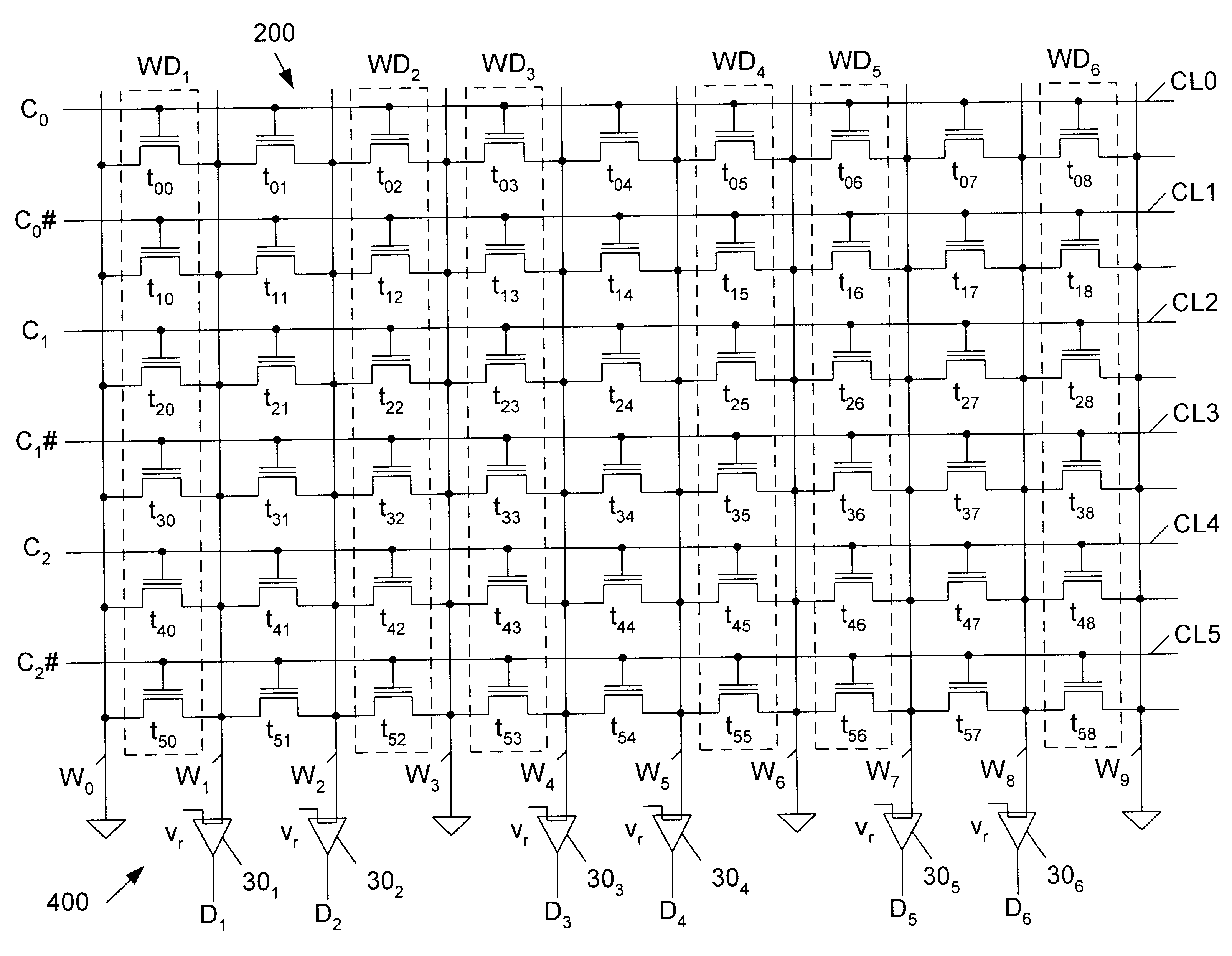
Consequently, three columns of memory transistors are effectively used to store two columns of data, thereby making the overall efficiency of the NVCAM array equal to three transistors / bit.

Problems solved by technology

While it is relatively easy to implement a CAM structure for a conventional non-volatile memory array that implements a common-source configuration, the task becomes more complex for a non-volatile memory array that implements a virtual-ground configuration.

Method used


Image

  • Content-addressable memory for virtual ground flash architectures
  • Content-addressable memory for virtual ground flash architectures
  • Content-addressable memory for virtual ground flash architectures

Examples


first embodiment

The first embodiment of the present invention will now be described in detail, with reference to FIG. 4.

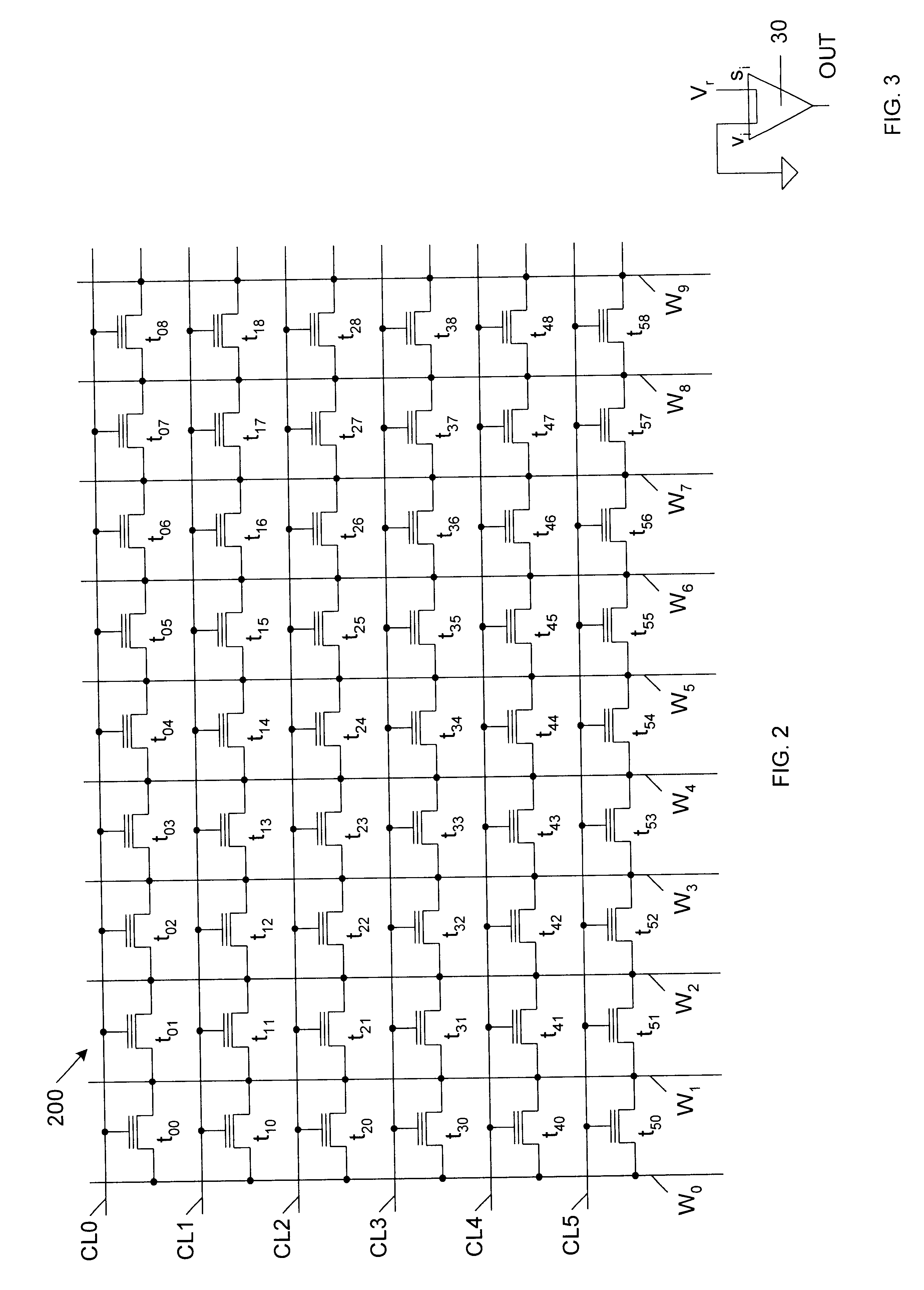
FIG. 4 is a circuit diagram of a non-volatile content addressable memory (NVCAM) 400, which is implemented using array 200 (FIG. 2). Compare lines CL0-CL5 are coupled to receive compare bits C0-C0#, C1-C1# and C2-C2#, respectively. Word lines W0, W3, W6 and W9 are connected to receive a ground supply voltage (GND). Word lines W1, W2, W4, W5, W7 and W8 are coupled to the s.sub.i input terminals of sense amplifiers 30.sub.1 -30.sub.6, respectively. The v.sub.i input terminals of sense amplifiers 30.sub.1 -30.sub.6 are coupled to receive a reference voltage v.sub.r of about 2 Volts. Sense amplifiers 30.sub.1 -30.sub.6 provide output signals D1-D6, respectively.

In the first embodiment, the number of words in NVCAM array 400 is equal to the number of word lines minus one, times 2 / 3 (e.g., 2 / 3.times.(10-1)=6 words), and the number of bits per word is equal to 1 / 2 of the number of compar...

second embodiment

A second embodiment of the present invention will now be described. Like the first embodiment, the second embodiment can use either conventional floating gate non-volatile memory transistors or 2-bit non-volatile memory transistors (with only one bit of the 2-bit non-volatile memory transistors being used).

FIG. 5 is a circuit diagram of a non-volatile content addressable memory (NVCAM) 500, which is implemented using array 200 (FIG. 2). Compare lines CL0-CL5 are coupled to receive compare bits C0-C0#, C1-C1# and C2-C2#, respectively. Word lines W1, W5 and W9 are connected to receive a ground supply voltage (GND). Word lines W0, W2, W3, W4, W6, W7 and W8 are coupled to the s.sub.i input terminals of sense amplifiers 50.sub.1 -50.sub.7, respectively. Sense amplifiers 50.sub.1 -50.sub.7 provide output signals to logic blocks LB.sub.1 -LB.sub.9 as illustrated. Each of sense amplifiers 50.sub.1 -50.sub.7 is identical to sense amplifier 30 (FIG. 3). Each of logic blocks LB.sub.1 -LB.sub.9...

third embodiment

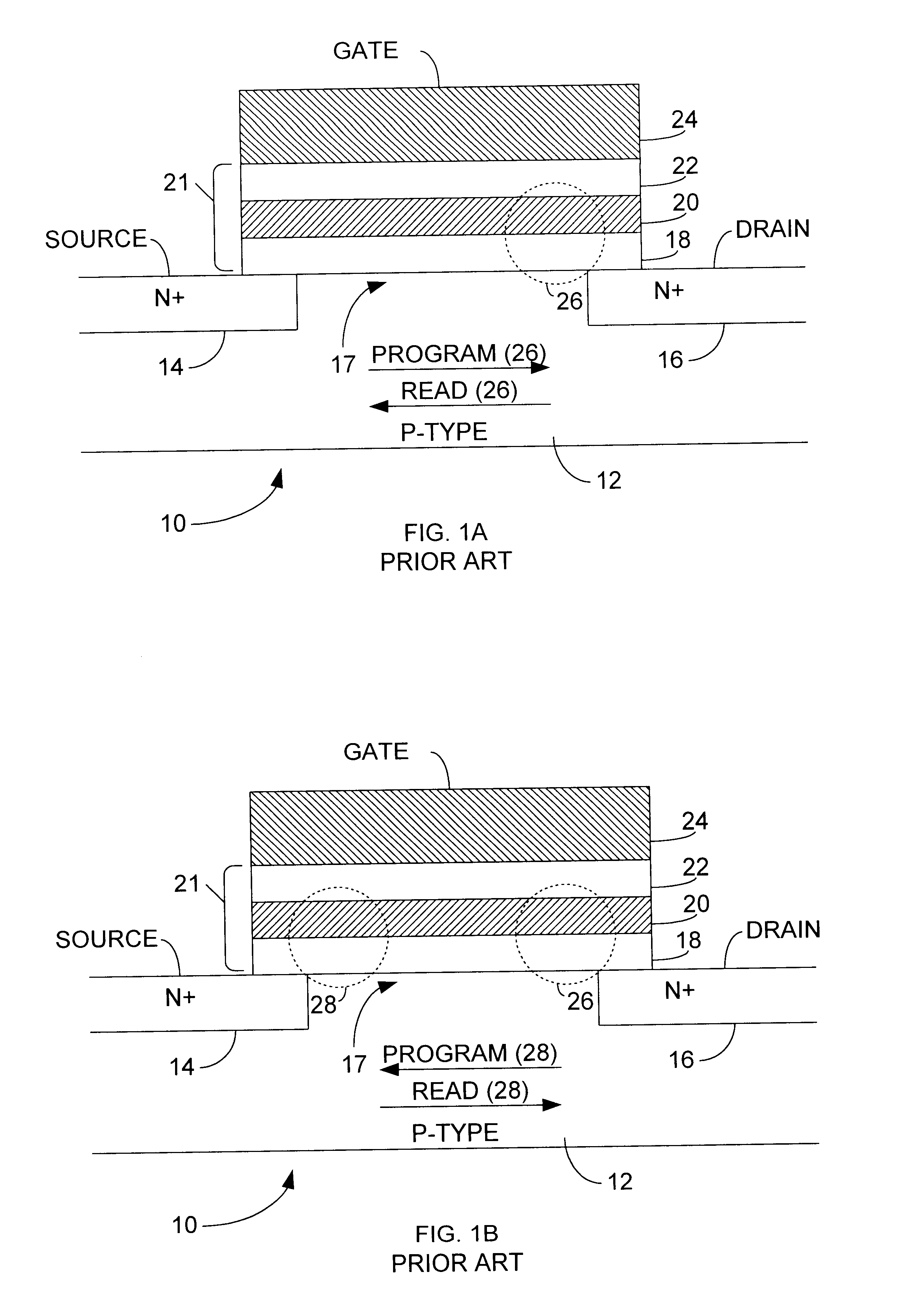
A third embodiment of the present invention will now be described. It should be noted that the first and second embodiments can use either conventional floating gate non-volatile memory transistors or 2-bit non-volatile memory transistors (with only one bit of the 2-bit non-volatile memory transistors being used). In contrast, the third embodiment requires 2-bit non-volatile memory transistors, which include left and right charge trapping regions that can be independently programmed and read as described above in FIGS. 1A and 1B. It is one purpose of the third embodiment to utilize two bits per storage device, thereby multiplying the density of the resulting NVCAM array two-fold as compared to the first embodiment. In accordance with the third embodiment, array 200 is able to support six 6-bit words (as compared with six 3-bit words in the first embodiment).

FIG. 6 is a circuit diagram of a NVCAM array 600 in accordance with the third embodiment of the present invention. NVCAM array ...


PUM


Abstract

Five architectures for the implementation of virtual ground non-volatile content-addressable memory are provided. Three of the architectures are applicable to 2-bit non-volatile memory transistors having separate programming capability for two current directions (i.e., drain-to-source and source-to-drain. Another architecture is applicable to any floating gate memory transistor, including 1-bit and 2-bit non-volatile memory transistors. In general, an array of non-volatile memory transistors is arranged in a plurality of horizontal rows and vertical columns. Words are stored in selected columns of the array. Horizontal compare lines are coupled to receive a comparand word, with each compare line being coupled to the gates of the memory transistors in a row of the array. The vertically aligned source / drain regions of the memory transistors are coupled to form word lines. Sense amplifiers are coupled to selected word lines. Switches can be coupled to the sense amplifiers and / or word lines, thereby enabling program and compare operations to be performed in two different directions when 2-bit non-volatile memory transistors are used. Compare operations can be performed over two or more phases when 2-bit non-volatile memory transistors are used. Sequential logic circuits can also be coupled to the sense amplifiers, and used to store the results of different compare phases.

Description

1. Field of the InventionThe present invention relates to a non-volatile content-addressable memory (NVCAM) array implemented using a virtual-ground flash memory architecture.2. Description of Related ArtContent-addressable memory (CAM) arrays are used in various applications where a fast searching capability is needed. Non-volatile CAM (NVCAM) arrays form a sub-class within this family. One example of a NVCAM array is described in U.S. Pat. No. 5,808,929.While it is relatively easy to implement a CAM structure for a conventional non-volatile memory array that implements a common-source configuration, the task becomes more complex for a non-volatile memory array that implements a virtual-ground configuration. For example, U.S. Pat. No. 5,917,743 requires eight transistors to form a CAM cell and, in addition, requires the fabrication of a special isolation device.It would therefore be desirable to have a NVCAM structure having a virtual-ground configuration that overcomes the deficie...

Claims


Application Information

Patent Timeline
IPC IPC(8): G11C15/00G11C16/04G11C11/56G11C15/04H01L21/28H01L21/8239H01L21/8246H01L27/105
CPCG11C11/5671G11C15/046G11C16/0475H01L27/1052H01L27/105H01L21/28282H01L27/11568H01L29/40117H10B99/00H10B43/30
Inventor LAVI, YOAV
Owner LONGITUDE LICENSING LTD
Learn More