

SRAM operating with a reduced power dissipation
a technology of sram and power dissipation, applied in the direction of logic circuit coupling/interface arrangement, digital storage, instruments, etc., can solve the problems of large chip area, small off-leak current difference,
- Summary
- Abstract
- Description
- Claims
- Application Information
AI Technical Summary
Problems solved by technology
Method used
Image

Examples
first embodiment
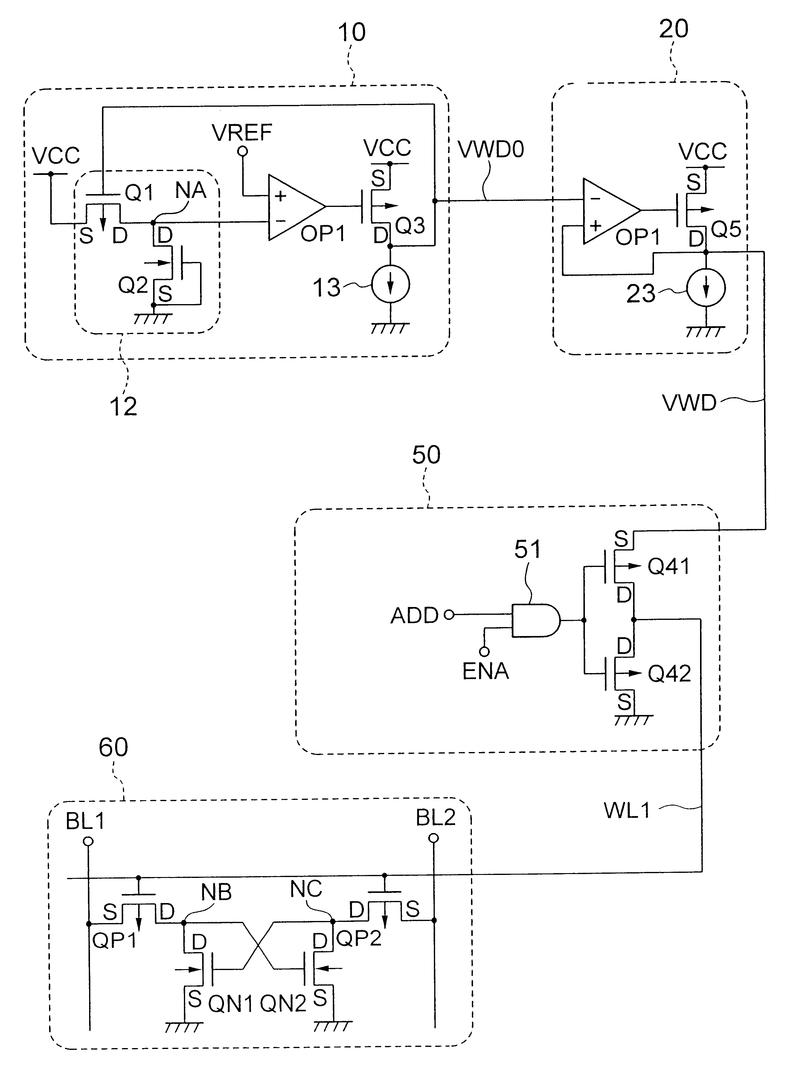
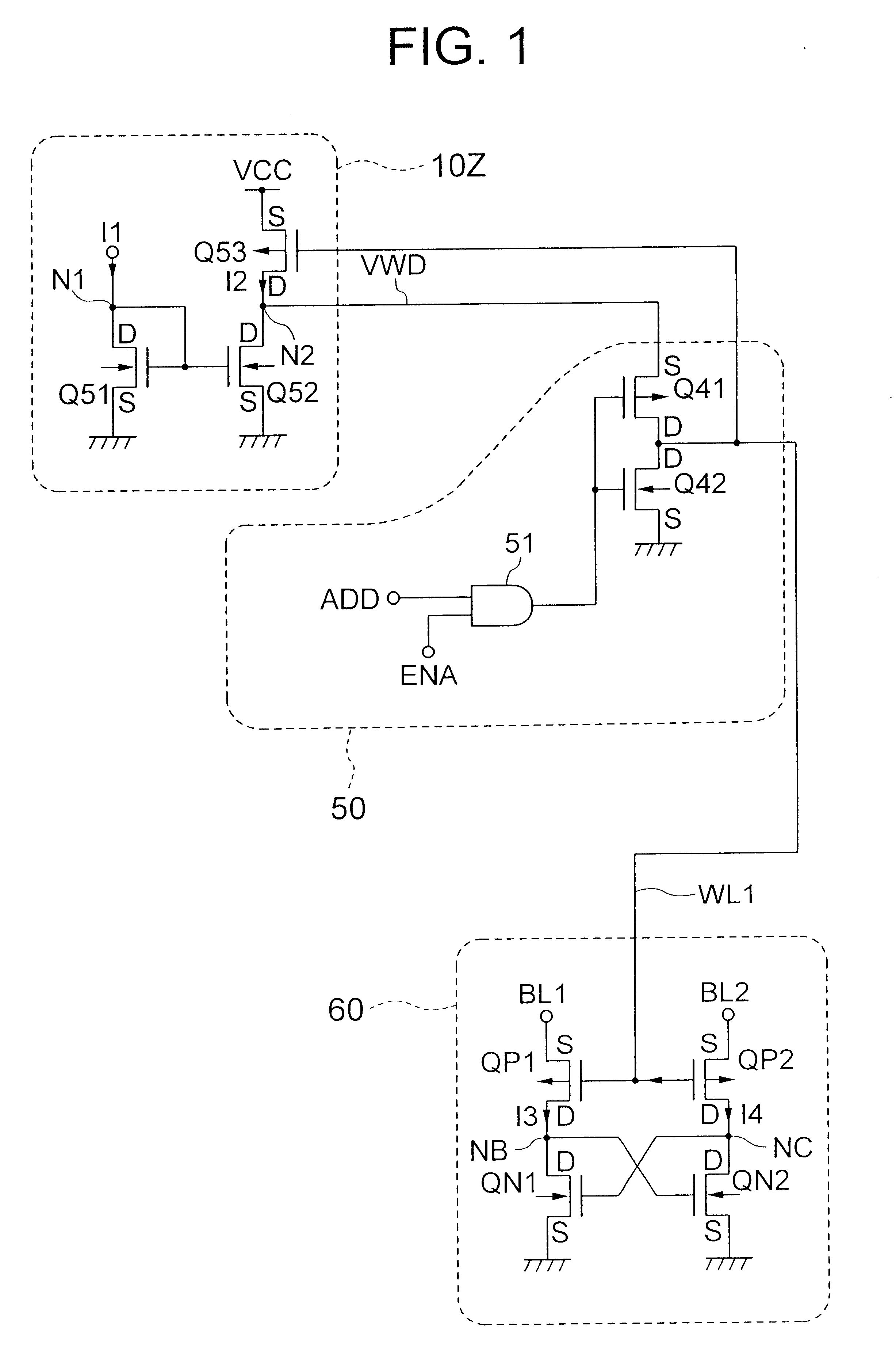
Referring to FIG. 3, a SRAM according to the present invention includes a single reference voltage generator 10 for generating a reference precharge voltage VWD0, a single impedance converter 20 for receiving the reference precharge voltage VWD0 to generate a precharge voltage VWD with a lower internal impedance, a plurality of word line drivers 50 each disposed corresponding to a word line WL1 and switching the corresponding word line WL1 between the ground potential and the precharge voltage level VWD, a plurality of memory cells 60 arranged in a matrix, and a plurality of pairs of bit lines BL1 and BL2 each disposed for a corresponding column of the memory cells,. Each row of memory cells is activated by a corresponding word line driver 50, and one of the memory cells in the row receives / delivers data through a corresponding pair of bit lines BL1 and BL2, the potentials of which depend on the data to be received or delivered.
Each memory cell 60 includes a pair of transfer pMOS tr...
fourth embodiment
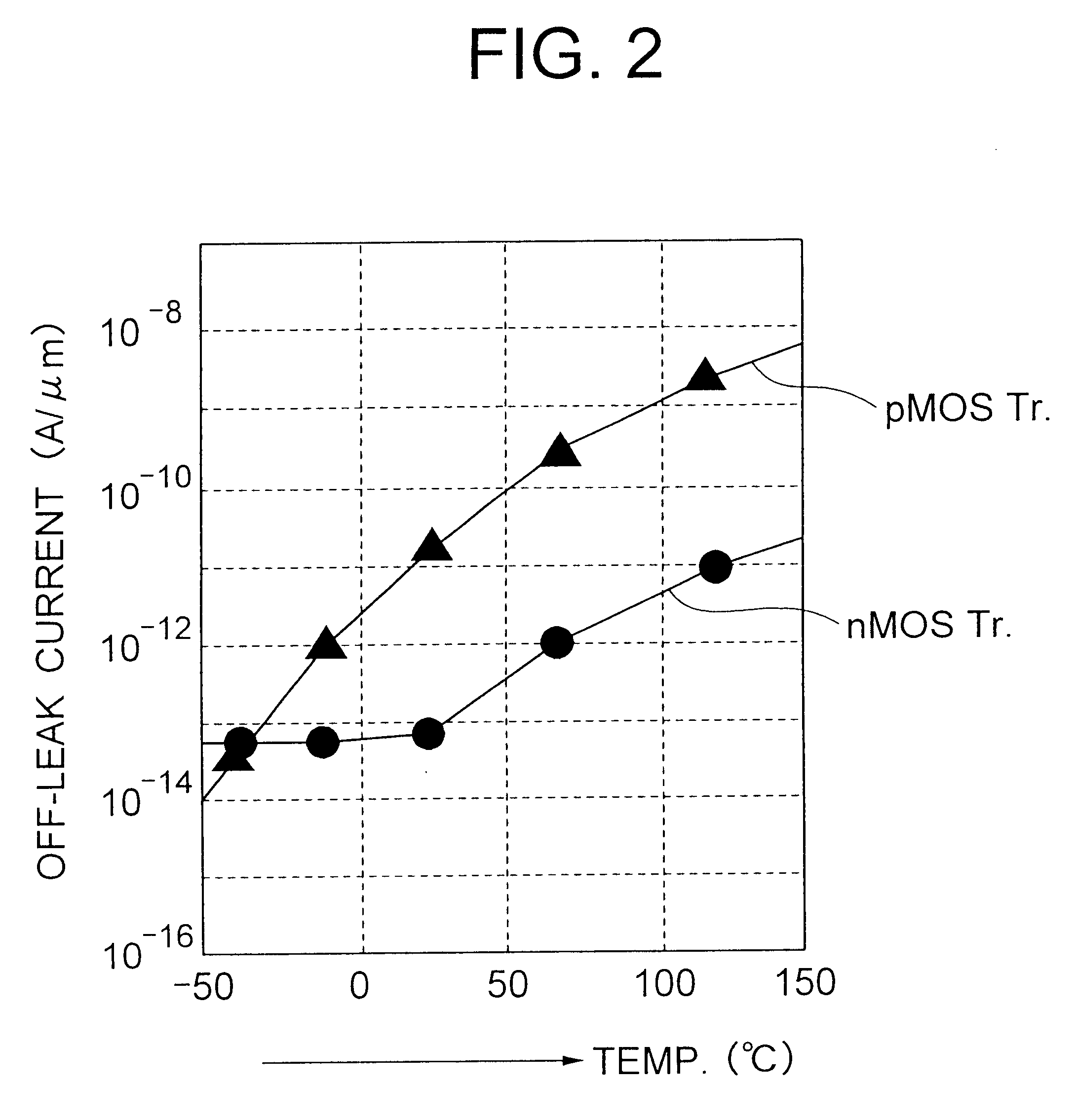
Referring to FIG. 6, a reference voltage generator 10C in a SRAM according to the present invention includes a pMOS transistor Q1 having a source connected to the VCC source line and a plurality of (N in number) nMOS transistors Q2 connected in parallel between pMOS transistor Q1 and the ground, with the gates of nMOS transistors Q2 being connected to the ground. The drains of pMOS transistor Q1 and nMOS transistors Q2 are connected together for delivering a reference precharge voltage VWD0. The number "N" may be 100 or more, whereby the "off-leak current ratio" between the pMOS transistor and the nMOS transistor may be two orders in magnitude in a decimal notation. The plurality of nMOS transistors function as load resistors.
The reference voltage generator 10C in the present embodiment achieves a simple structure and has an excellent temperature characteristic. In addition, internal reference voltage is not needed.
Referring to FIG. 7, a SRAM according to a fifth embodiment of the p...
sixth embodiment
Referring to FIG. 8, an impedance converter 20B used in a SRAM according to the present invention is similar to the impedance converter 20A except that each of the level converters 24 and 25 in the present embodiment has a control input CNT1 or CNT2, through which a control signal for selecting the conversion ratio or voltage drop of the level converter 24 or 25 is input. The level converters 24 and 25 may have different voltage drops instead of different conversion ratios.
After an operational test for a final product of the SRAM, the control signals are selected based on the test results to select suitable conversion ratios, to thereby improve the characteristics of operational amplifier OP2 and achieves a stable precharge operation as well as reduction of the power dissipation.
Referring to FIG. 9, a SRAM according to a seventh embodiment of the present invention is similar to the first embodiment except that a plurality of reference voltage generators 10 are provided for a single ...
PUM
 Abstract
Description
Claims
Application Information