Method and apparatus for characterizing semiconductor device performance variations based on independent critical dimension measurements

a technology of critical dimension and measurement method, applied in the field of semiconductor device performance variation based on independent critical dimension measurement, can solve the problems of complex digital circuit, such as microprocessors, and the demand for fast-switching transistors

Inactive Publication Date: 2002-02-12
ADVANCED MICRO DEVICES INC
View PDF7 Cites 113 Cited by
  • Summary
  • Abstract
  • Description
  • Claims
  • Application Information

AI Technical Summary

Problems solved by technology

In particular, complex digital circuits, such as microprocessors and the like, demand fast-switching transistors.
Due to the small length of the gate electrode, which usually consists of a doped polycrystalline silicon, the electrical resistance of the gate electrode is relatively high, and it may cause high RC-delay time constants.
Hence, the transverse electrical field necessary for fully opening the channel is delayed, thereby further deteriorating the switching time of the transistor line.
If a gate electrode is formed overly large, its switching speed is compromised.
On the other hand, if the gate electrode is formed too small, based on the design characteristics of the adjacent dielectric materials, the transistor will exhibit a higher leakage current, causing an excessive power usage and heat generation.
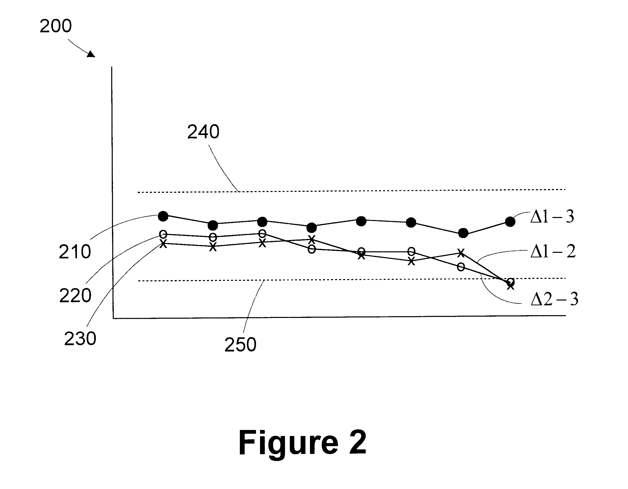
The metrology tools (e.g., scanning electron microscope) used to perform the critical dimension metrology are extremely sensitive.
Even with such oversight, it is possible for the metrology tool to drift, thus resulting in a drift in the critical dimension measurements.
Adjusting the process based on errant deviations caused by metrology drifts may actually increase the variation in the gate electrode critical dimensions.
For example, the errant metrology tool may improperly indicate that the gate electrodes are too large.
The process may be adjusted to further reduce the gate electrode length, resulting in the formation of gate electrodes that are actually too small.
When the devices reach the point where they can be electrically tested, they may have excessive leakage and perform poorly, depending on the magnitude of the errant length reduction.

Method used


Image

  • Method and apparatus for characterizing semiconductor device performance variations based on independent critical dimension measurements
  • Method and apparatus for characterizing semiconductor device performance variations based on independent critical dimension measurements
  • Method and apparatus for characterizing semiconductor device performance variations based on independent critical dimension measurements

Examples


Embodiment Construction

Illustrative embodiments of the invention are described below. In the interest of clarity, not all features of an actual implementation are described in this specification. It will of course be appreciated that in the development of any such actual embodiment, numerous implementation-specific decisions must be made to achieve the developers' specific goals, such as compliance with system-related and business-related constraints, which will vary from one implementation to another. Moreover, it will be appreciated that such a development effort might be complex and time-consuming, but would nevertheless be a routine undertaking for those of ordinary skill in the art having the benefit of this disclosure.

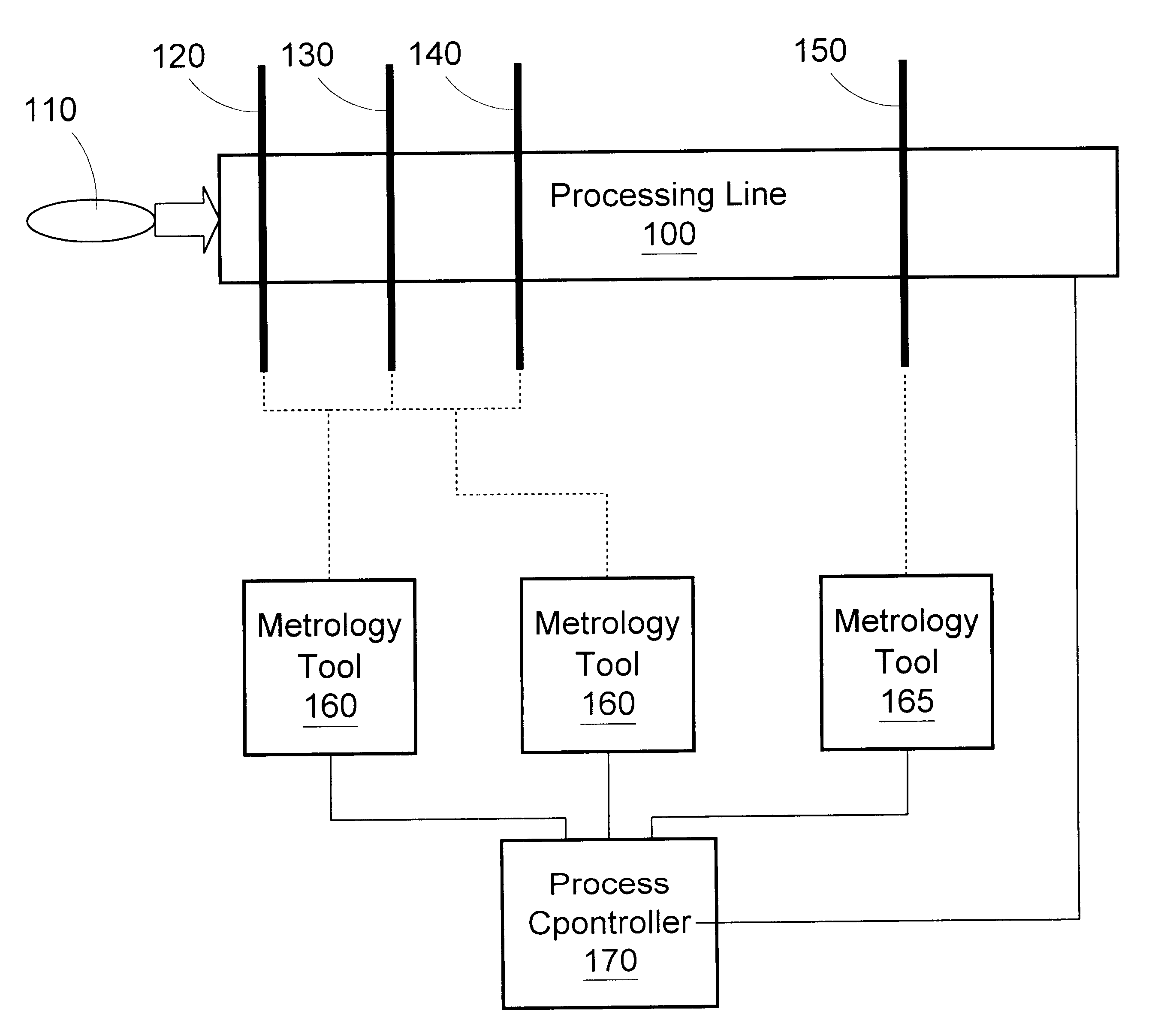
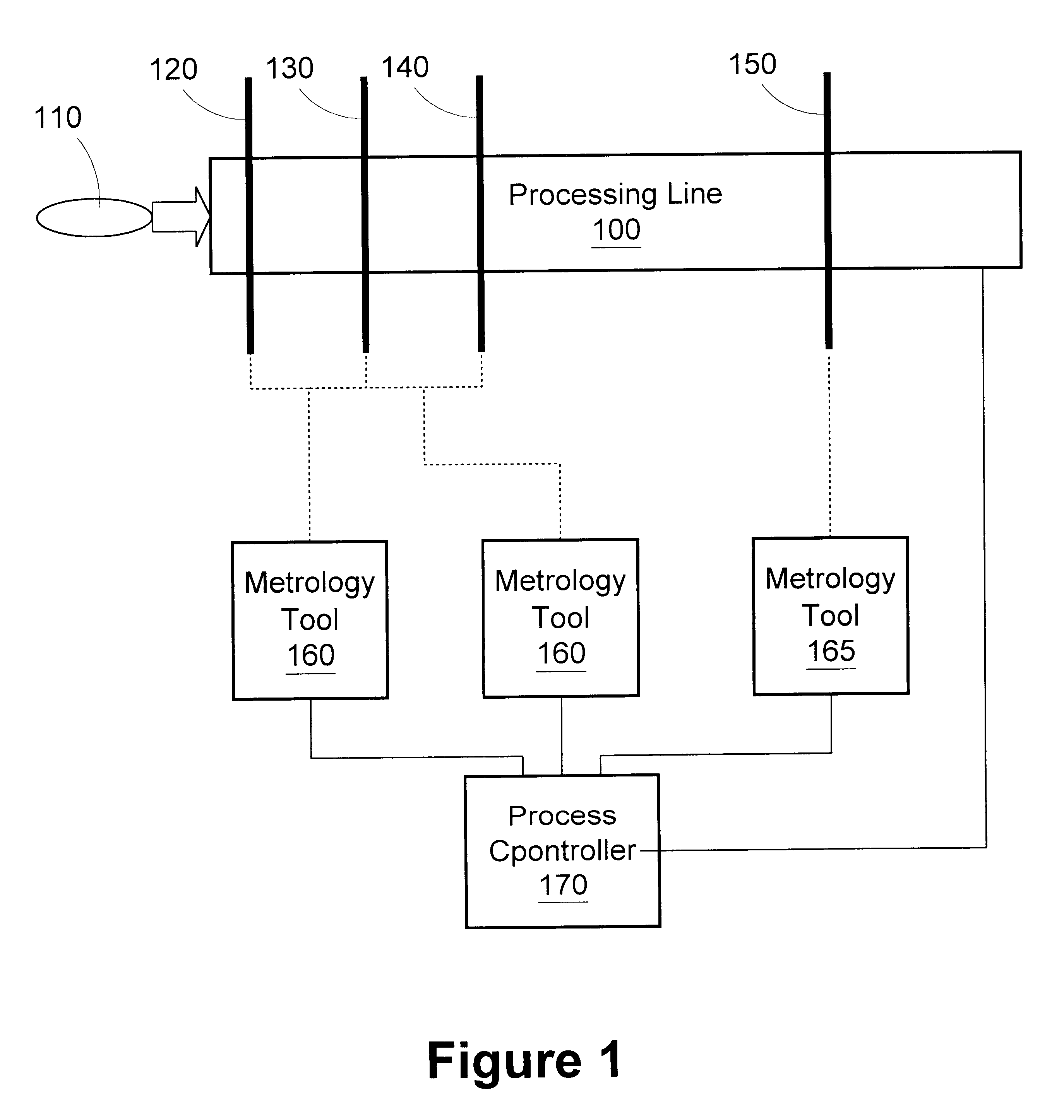
Referring now to FIG. 1, a simplified block diagram of a portion of an illustrative processing line 100 for processing wafers 110 in accordance with one embodiment of the present invention is provided. The processing line 100 comprises a plurality of tools used in a process flow for fo...


PUM


Abstract

A method for characterizing semiconductor device performance variations includes processing a wafer in a processing line to form a feature on the wafer; measuring a physical critical dimension of the feature in a first metrology tool to generate a first critical dimension measurement; measuring the physical critical dimension of the feature in a second metrology tool to generate a second critical dimension measurement independent of the first critical dimension measurement; determining an effective critical dimension of the feature in a third metrology tool to generate a third critical dimension measurement; and comparing the first, second, and third critical dimension measurements to identify a metrology drift in one of the first and second metrology tools. A system for characterizing semiconductor device performance variations includes a processing line, first, second, and third metrology tools, and a process controller. The processing line is adapted to process a wafer to form a feature on the wafer. The first metrology tool is adapted to measure a physical critical dimension of the feature to generate a first critical dimension measurement. The second metrology tool is adapted to measure the physical critical dimension of the feature to generate a second critical dimension measurement independent of the first critical dimension measurement. The third metrology tool adapted to determine an effective critical dimension of the feature to generate a third critical dimension measurement. The process controller is adapted to compare the first, second, and third critical dimension measurements to identify a metrology drift in one of the first and second metrology tools.

Description

1. Field of the InventionThis invention relates generally to the field of semiconductor processing and, more particularly, to a method and apparatus for characterizing semiconductor device performance variations based on independent critical dimension measurements.2. Description of the Related ArtSemiconductor integrated circuit devices are employed in numerous applications, including microprocessors. Generally, the performance of a semiconductor device is dependent on both the density and the speed of the devices formed therein. A common element of a semiconductor device that has a great impact on its performance is a transistor. Design features, such as gate length and channel length, are being steadily decreased in order to achieve higher package densities and to improve device performance. The rapid advance of field effect transistor design has affected a large variety of activities in the field of electronics in which the transistors are operated in a binary switching mode. In ...

Claims


Application Information

Patent Timeline
Patent Type & Authority Patents(United States)
IPC IPC(8): H01L21/66
CPCH01L22/26H01L22/12
Inventor TOPRAC, ANTHONY J.WRISTERS, DERICK J.CHEEK, JON D.
Owner ADVANCED MICRO DEVICES INC
Why Eureka
Try Eureka