EMC characteristics of a printed circuit board

a printed circuit board and characteristics technology, applied in the direction of line-transmission details, association of printed circuit non-printed electric components, electrical apparatus construction details, etc., can solve the problems of less and less practicability of the structure illustrated in figs. 1, 2a, and 2b, and achieve the effect of minimizing the impedance encountered and minimizing the flow of curren

Inactive Publication Date: 2002-02-19
DELL PROD LP
View PDF4 Cites 36 Cited by
  • Summary
  • Abstract
  • Description
  • Claims
  • Application Information

AI Technical Summary

Benefits of technology

FIG. 5A depicts split conducting plane 516 wherein the split is depicted as repeating rectangular structure dielectric-filled moat 500 which substantially minimizes an impedance encountered by return current 360 and which substantially minimizes the flow of current at or near peripheries 404, 406 of split conducting plane 516 such as multilayer printed circuit board structure 300.

Problems solved by technology

Unfortunately, as printed circuit board densities have increased, the structure illustrated in FIGS. 1, 2A, and 2B is becoming less and less practicable.

Method used


Image

  • EMC characteristics of a printed circuit board
  • EMC characteristics of a printed circuit board
  • EMC characteristics of a printed circuit board

Examples


Embodiment Construction

)

The following sets forth a detailed description of the best contemplated mode for carrying out the independent invention(s) described herein. The description is intended to be illustrative and should not be taken to be limiting.

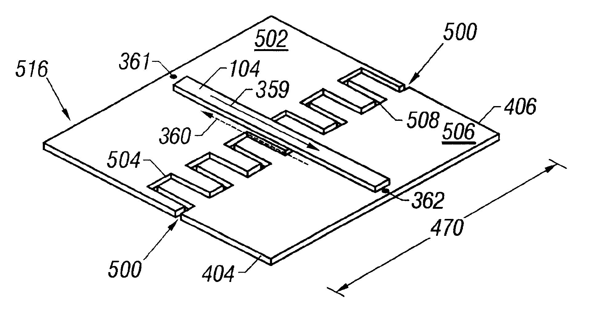
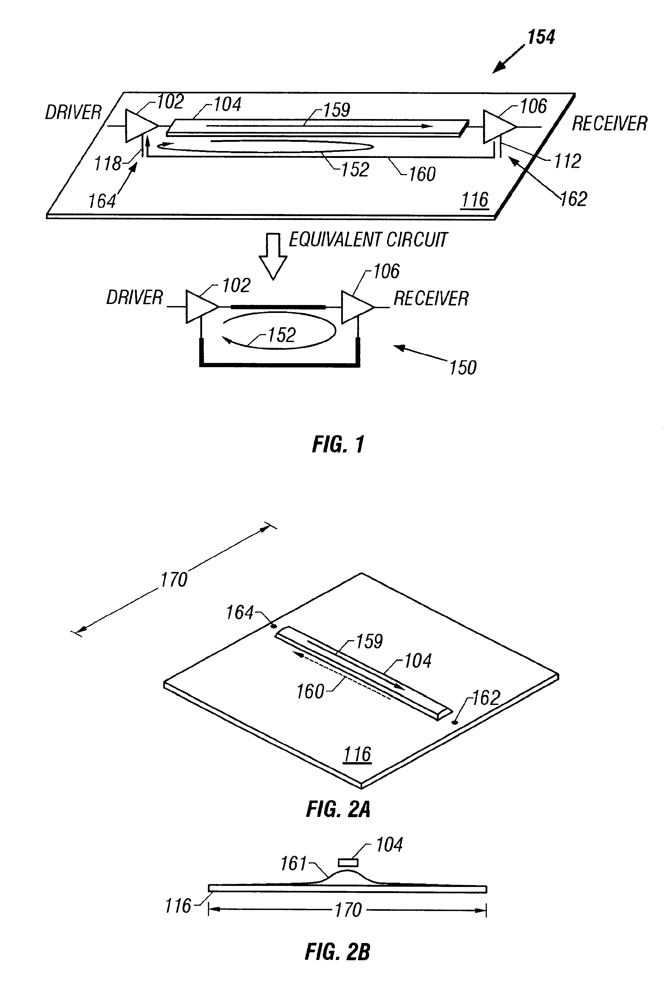
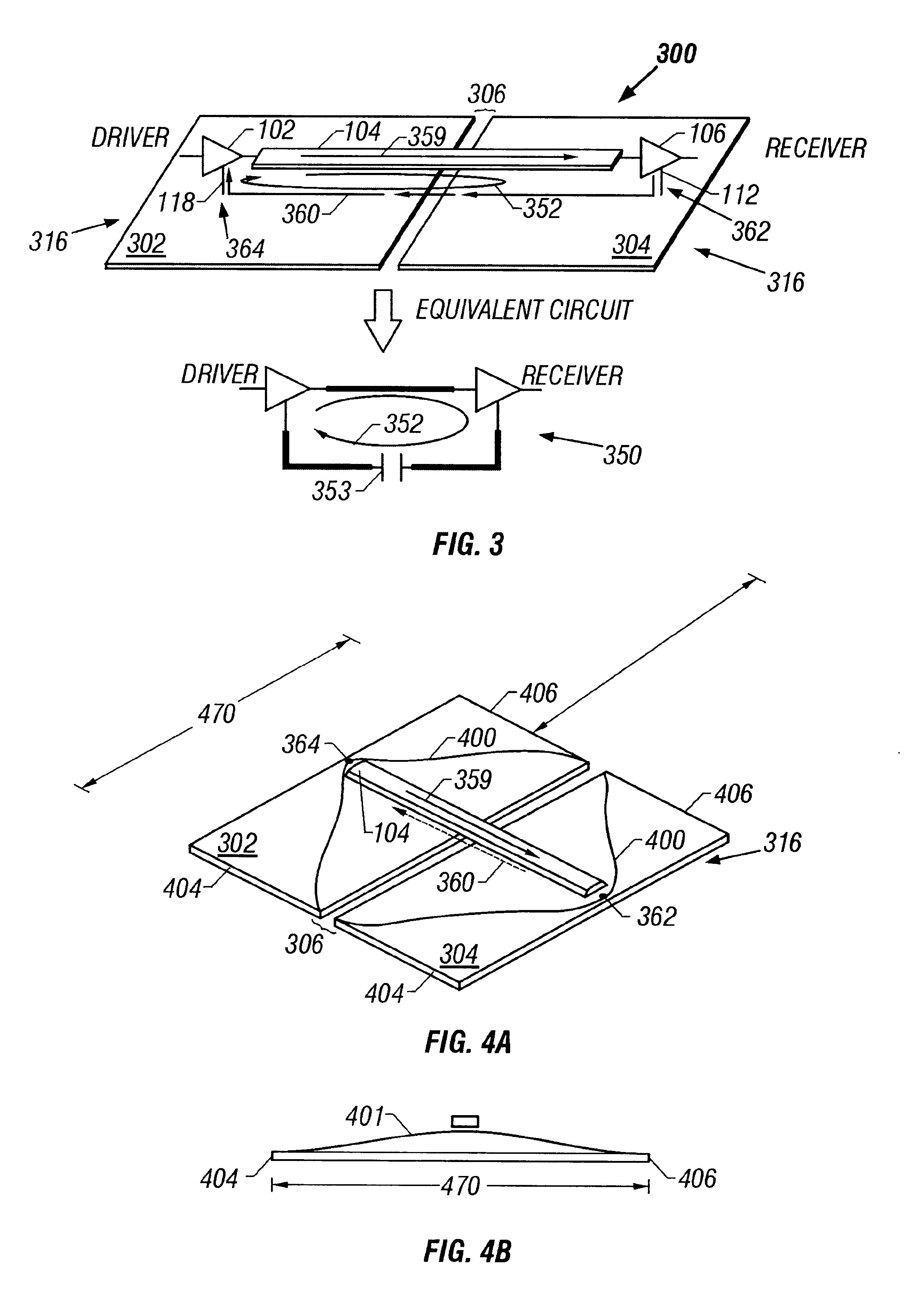
With reference now to FIG. 4A, depicted is an isolated perspective view of first metallic conducting part 302 separated from second metallic conducting part 304 by dielectric-filled moat 306 of FIG. 3. Because there is no longer a physically contiguous path such as in metallic conducting plane 116 (of FIG. 1), return current 360, seeking the path of least impedance will tend to spread out and follow fan-shaped current flow path 400 (where the flow path has current distribution 401 shown in FIG. 4B, below) from point 162 to point 164. Those skilled in the art will recognize that there are a multitude of ways in which this current behavior can be described, but one grossly-simplified way would be to recognize that for a parallel plate capacitor, the capacitanc...


PUM


Abstract

An apparatus for use with data processing systems. The apparatus provides a split metallic conducting plane having a split formed by a substantially-dielectric-filled moat spanning a width of a side of a first metallic conducting part running substantially parallel to a side of a second metallic conducting part, with the moat structured such that the side of the first metallic part has at least two indentations and such that the side of the second metallic part has at least two indentations, and where a metallic trace is located proximate to the split metallic conducting plane.

Description

1. Field of the InventionThe present invention relates, in general, to printed circuit boards.2. Description of the Related ArtA printed circuit board is a board made of non-conducting material, such as plastic, glass, ceramic, or some other dielectric on which chips and other electronics are mounted. A multilayer printed circuit board is a printed circuit board consisting of two or more layers of board material. Each separate layer has its own metallic tracings to provide electrical connections between various electronic components and to provide connections to other layers. The layers are laminated together to produce a single circuit board to which the components, such as integrated circuits, resistors, and capacitors are attached.One common multilayer printed circuit board scenario is to have alternating layers, where a first layer is composed in all or part of conducting materials, a second layer is composed mostly of insulating material, and a third layer is composed in all or...

Claims


Application Information

Patent Timeline
Patent Type & Authority Patents(United States)
IPC IPC(8): H05K1/02
CPCH05K1/0216H05K2201/09663H05K2201/093H05K2201/09245
Inventor HAILEY, JEFFERY C.
Owner DELL PROD LP
Why Eureka
Try Eureka