Photodiode

a photodiode and image sensor technology, applied in semiconductor devices, radio frequency control devices, electrical equipment, etc., can solve the problems of increasing noise during photosensing measurement, reducing the stability of the photodiode cmos image sensor, and non-uniform distribution of electrical field in the photodiode array, so as to reduce current leakage phenomenon, reduce read noise, and improve quality. reliability

Inactive Publication Date: 2002-02-26
UNITED MICROELECTRONICS CORP
View PDF8 Cites 33 Cited by
  • Summary
  • Abstract
  • Description
  • Claims
  • Application Information

AI Technical Summary

Benefits of technology

As described above, in the photodiode provided by this invention, the dummy isolation layer is used to separate the second conductive type heavily doped region and the isolation layer. If LOCOS is performed on the isolation layer to form an oxide layer, and bird's beak dislocation phenomenon appears at a peripheral of the oxide layer. The photodiodes still would not leak current because of the dummy isolation layer. Moreover, since the width of the dummy isolation layer is far less than that of the isolation layer. If LOCOS is performed on the dummy isolation layer to form an oxide layer, the bird's beak is too small to cause significant dislocation (current leakage) phenomenon. Concerning the photodiode array formed by the photodiodes, the first conductive type heavily doped region of each of the photodiodes can be connected to ground individually. This is unlike the conventional photodiode array that has ground connections at the two ends of a doped region only, electric field thus can be distributed more uniformly and pike field induced leakage path can be eliminated. As a result, the photodiode CMOS image sensor provided by this invention has lower read noise and higher quality reliability which are advantageous to mass production.
The photodiode, provided by this invention, further comprises a second conductive type lightly doped region located under the second conductive type heavily doped region. This is to further reduce current leakage phenomenon at the peripheral of the isolation layer. In addition, the photodiode provided by this invention may also comprise a first conductive type channel stop layer located under the isolation layer in the first conductive type doped substrate. This is to further reduce current leakage phenomenon at the peripheral of the isolation layer.

Problems solved by technology

Secondly, since the P-type heavily doped regions 150 for grounding purpose are located at the two ends of the photodiode array 102, this causes electric field distributing non-uniformly in the photodiode array 102.
These drawbacks increase noise during photosensing measurement and reduce stability of photodiode CMOS image sensor, thus are disadvantageous to mass production.

Method used


Image

  • Photodiode
  • Photodiode
  • Photodiode

Examples


Embodiment Construction

An n.sup.+ / p photodiode of a P-type substrate with an N-type doped region is used in this embodiment, but is not restrictive of the invention.

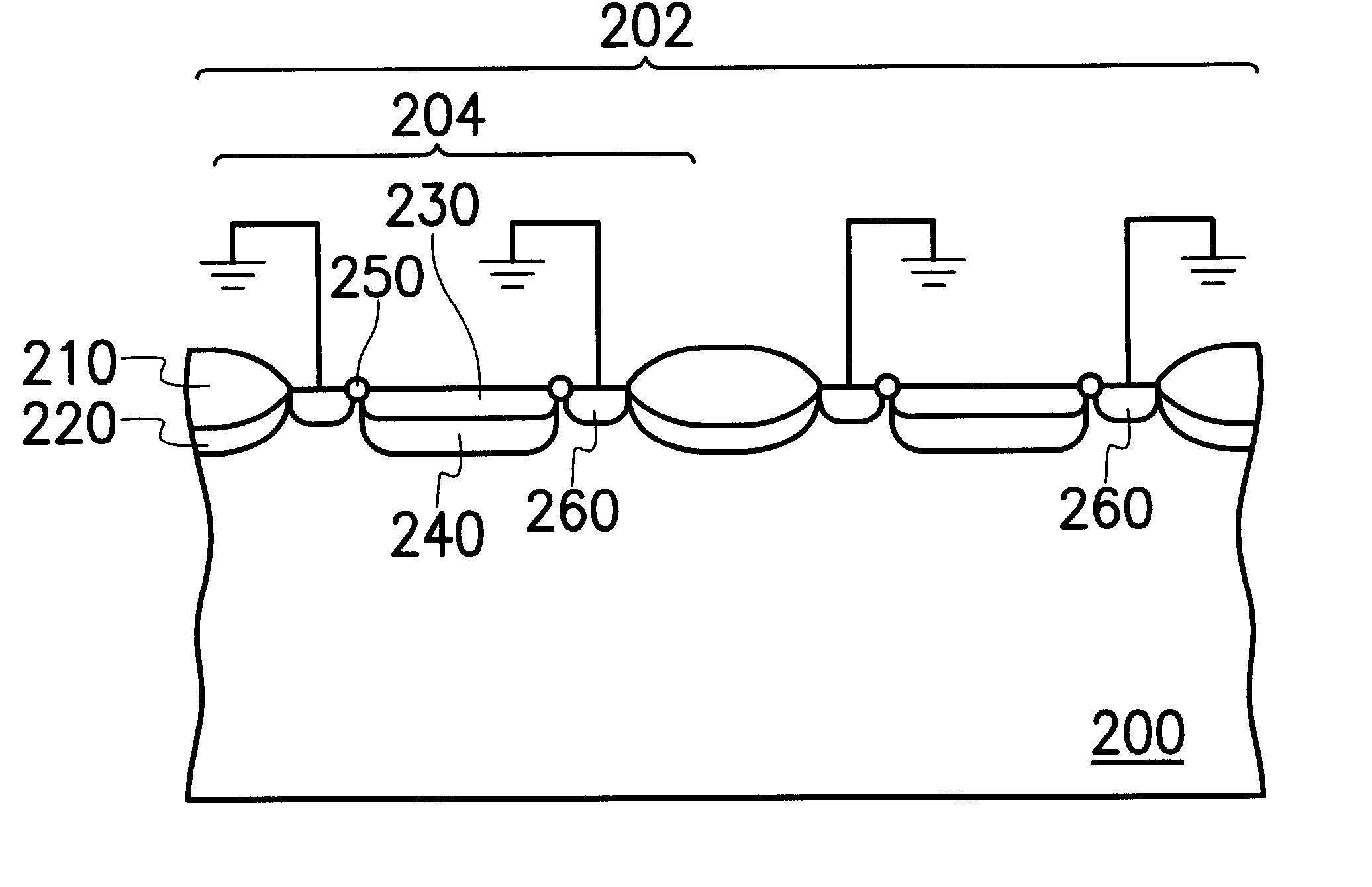
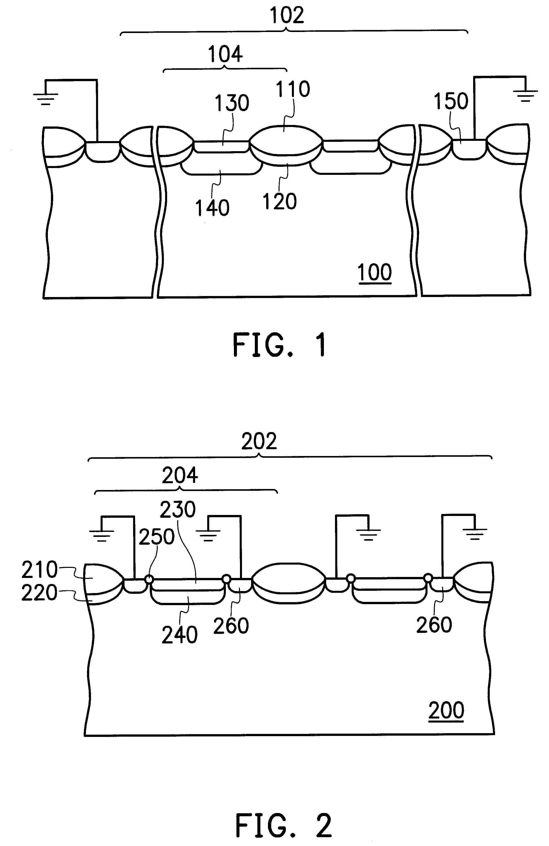
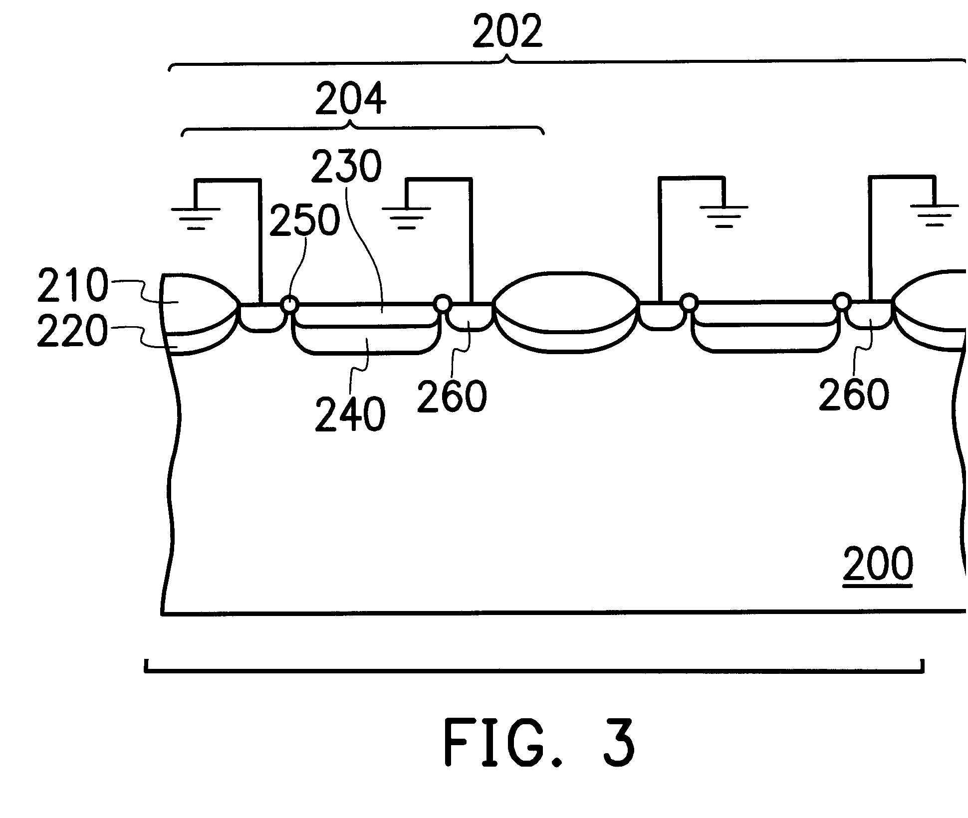
In FIG. 2, a cross sectional view of a photodiode array and a photodiode is shown. The photodiode array could be applied in a photodiode CMOS image sensor. As FIG. 2 illustrates, the photodiode array 202 is formed by several photodiodes 204. Each photodiode 204 comprises a P-type substrate 200, an N-type heavily doped region 230, an N-type lightly doped region 240, a dummy isolation layer 250, a P-type heavily doped region 260, an oxide layer 210 and a channel stop layer 220.

The N-type heavily doped region 230 is located in the P-type substrate 200 of which the doping concentration is lower than that of the N-type heavily doped region 230. The N-type lightly doped region 240 is located under the N-type heavily doped region 230, so that leakage current phenomenon at the peripheral of the oxide layer 210 can be further reduced. The dummy isolat...


PUM


Abstract

A photodiode. A second conductive type heavily doped region is located in a first conductive type doped substrate, and a dopant concentration of the second conductive type heavily doped region is larger than that of the first conductive type doped substrate. A dummy isolation is at a periphery of the second conductive type heavily doped region. A first conductive type heavily doped region is located at a periphery of the dummy isolation layer in the first conductive type doped substrate. A dopant concentration of the first conductive type heavily doped region is larger than that of the first conductive type substrate. An isolation layer is located at a periphery of the first conductive type doped region with a width much larger than that of the dummy isolation layer.

Description

This application claims the priority benefit of Taiwan application serial no. 89113125, filed Jul. 3, 2000.BACKGROUND OF THIS INVENTION1. Field of the InventionThis invention relates to a photosensitive device, and more particularly, to a photodiode and a photodiode complementary metal-oxide semiconductor (CMOS) image sensor.2. Description of Related Prior ArtPhotodiode image sensor is a widely applied image-sensing device. A typical photodiode image sensor comprises at least a reset transistor and a photodiode. Taking a photodiode with an N-type heavily doped region in a P-type substrate as an example, a voltage is applied to a gate of the reset transistor while operating the photodiode sensor. The reset transistor is thus switched on to charge a junction capacitor of this n.sup.+ / p photodiode. A large depletion region is induced with a reverse bias. When a specific potential is reached, the reset transistor is switched off. Once a light is impinged on the photosensitive region of...

Claims


Application Information

Patent Timeline
Patent Type & Authority Patents(United States)
IPC IPC(8): H01L27/146
CPCH01L27/14609H01L27/14689H01L27/1463
Inventor PAN, JUI-HSIANG
Owner UNITED MICROELECTRONICS CORP
Why Eureka
Try Eureka