FET-based, linear voltage-controlled resistor for wide-band gain control circuit

a wide-band gain control and linear technology, applied in the field of field-effect transistors, can solve the problems of non-zero common mode voltage, signal distortion in output signal v.sub.out through over-peaking, and gain control circuit of fig. 1 with significant limitations

Inactive Publication Date: 2002-03-12
CREDENCE SYSTEMS
View PDF6 Cites 6 Cited by
  • Summary
  • Abstract
  • Description
  • Claims
  • Application Information

AI Technical Summary

Problems solved by technology

Gain control circuit of FIG. 1 has some significant limitations.
First, the FET drain-to-source channel may have significant parasitic capacitance in parallel with the channel conductance, and the parasitic capacitance can cause signal distortion in output signal V.sub.OUT through over-peaking.
Another problem arises when the input signal V.sub.IN has a non-zero common mode voltage.
A symmetric FET is generally suitable for only relatively low frequency operation; high frequency FETs are typically asymmetric, but are not used as voltage-controlled resistors in differential gain control circuits because their asymmetry creates substantial harmonic distortion.
Thus when we want to provide a gain control circuit in a high frequency integrated circuit employing asymmetric FETs in other circuits, providing a symmetric FET for the gain control circuit becomes problematic.

Method used


Image

  • FET-based, linear voltage-controlled resistor for wide-band gain control circuit
  • FET-based, linear voltage-controlled resistor for wide-band gain control circuit
  • FET-based, linear voltage-controlled resistor for wide-band gain control circuit

Examples


Embodiment Construction

)

Dual FET Voltage-controlled Resistor

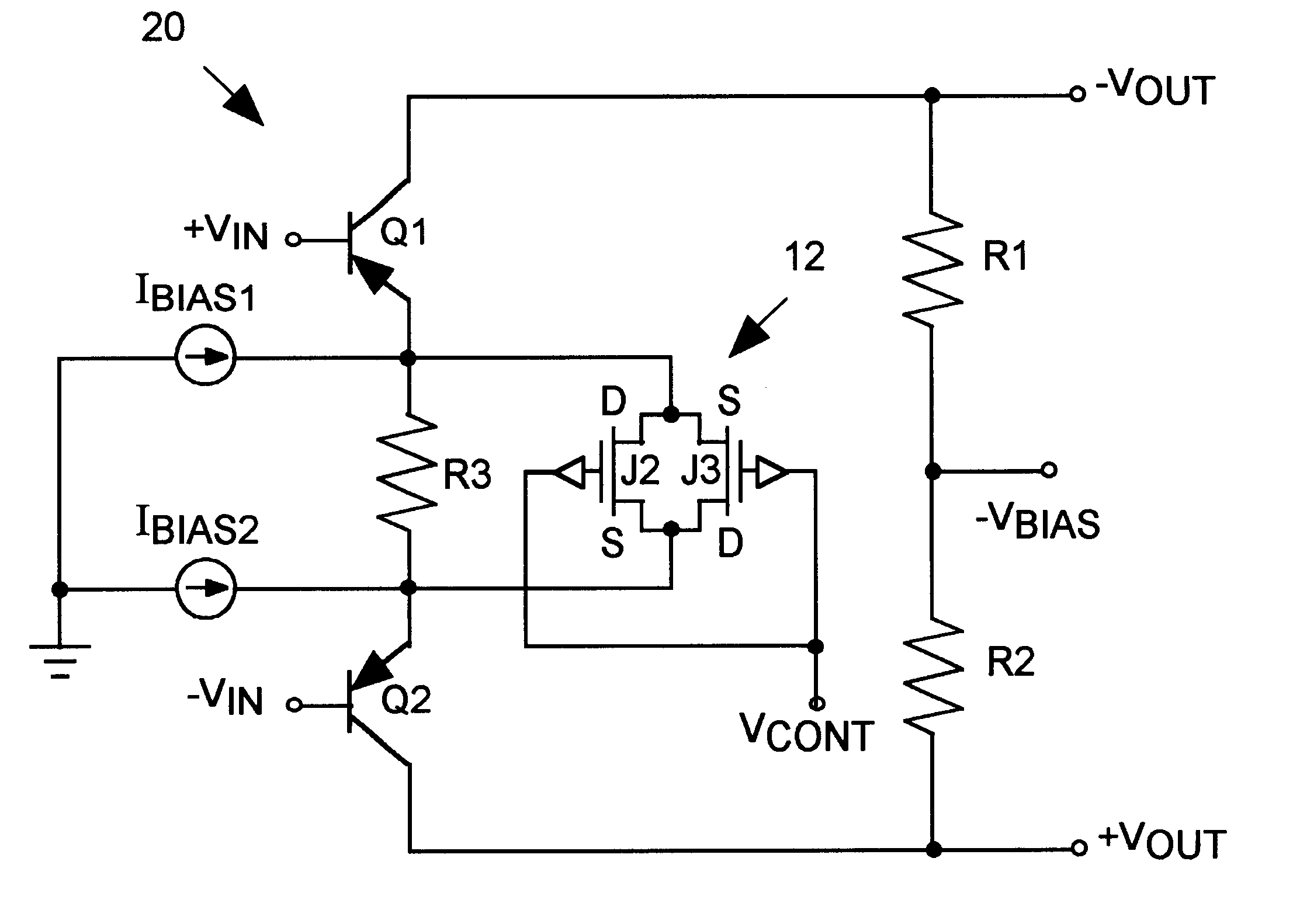
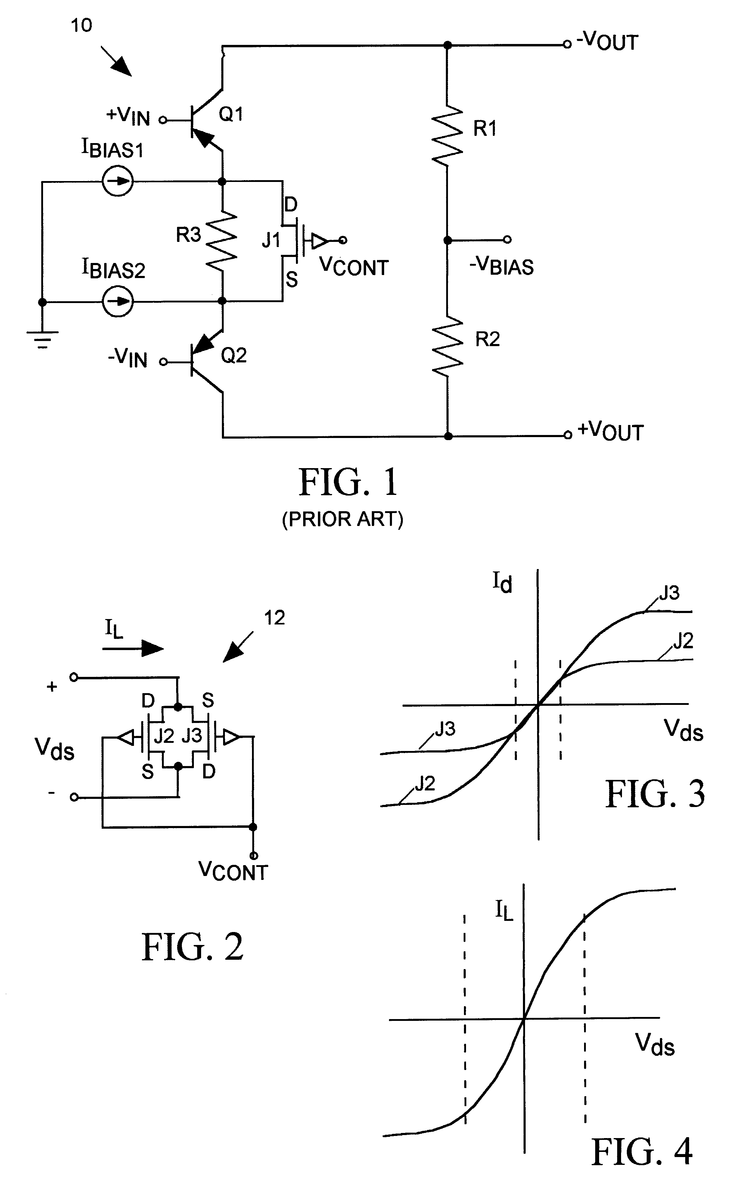
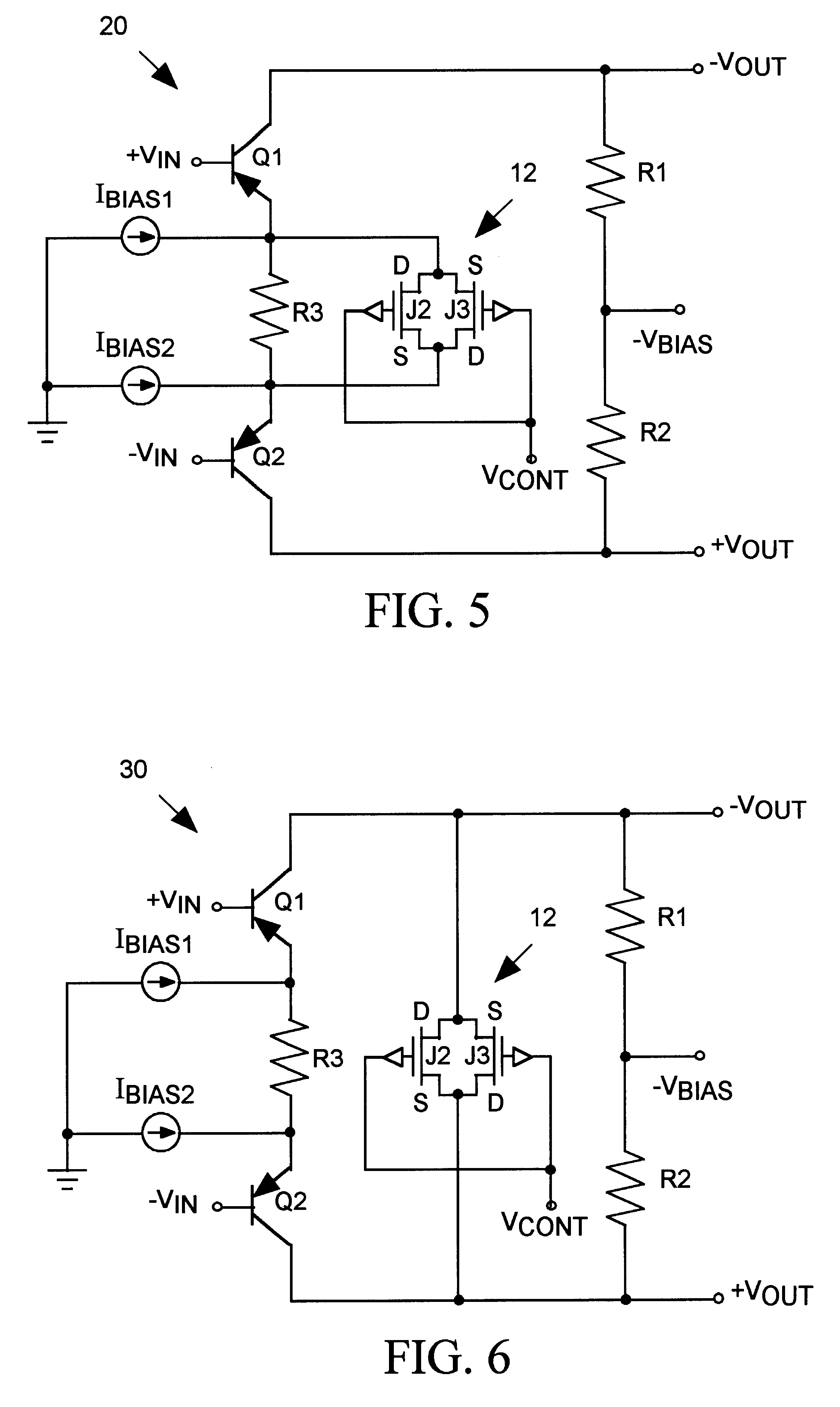
As illustrated in FIG. 2, a voltage-controlled resistor 12 in accordance with the invention is formed by two similar asymmetric field effect transistors (FETs) J2 and J3 connected drain-to-source. A control signal V.sub.CONT applied to the gates of FETs J2 and J3 controls their channel conductance, thereby controlling the relationship between a load current I.sub.L flowing through FETs J2 and J3 and a voltage V.sub.ds applied across their drain and sources terminals.

FIG. 3 plots of the drain currents I.sub.d of asymmetric transistors J2 and J3 as functions of V.sub.ds for some fixed voltage magnitude of control signal V.sub.CONT. We can see that the relationship between I.sub.d and V.sub.ds for each FET J2 and J3 is both linear and symmetrical, but only over a relatively narrow range of V.sub.ds about the V.sub.ds =0 axis.

FIG. 4 illustrates the load current I.sub.L of FIG. 2, the sum of the drain currents I.sub.d of transistors J2 and J3, as a fu...


PUM


Abstract

A gain control circuit for generating a differential output signal in response to a differential input signal with a gain controlled by an input control signal employs two asymmetric field effect transistors (FETs) as a linear, voltage-controlled resistor. The FETs are interconnected drain-to-source with the control signal being applied to their gates so that their combined channel current is a substantially linear and symmetric function of the input control signal voltage. The gain control circuit includes two bipolar transistors, with the differential input signal being applied across their bases and the differential output signal being developed across their collectors. A resistor links the emitters of the two transistors, sources are applied to the emitters, and a pair of resistors links each collector to a source of bias voltage. The FET-based voltage-controlled resistor may be connected either between the collectors or between the emitters of the two transistors. When connected between the collectors, output signal distortion due to any input signal common mode component is reduced.

Description

1. Field of the InventionThe present invention relates in general to the use of field effect transistors (FETs) as voltage-controlled resistors in gain control circuits, and in particular to the use of an FET-based voltage-controlled resistor in a continuously variable wide-band gain control circuit.2. Description of Related ArtA voltage-controlled resistor has a resistance that can be adjusted by an input control signal. Normally we want the current conducted by a voltage-controlled resistor be a linear function of the voltage across its load terminals. Thus while we want its resistance to be function of the voltage of a control signal applied to its control terminals, we do not want its resistance to vary with the voltage across its load terminals. Field effect transistors, particularly those fabricated using an "interdigitated" geometry, have long been used as voltage-controlled resistors because they exhibit a linear relationship between drain current I.sub.d and drain-to-source...

Claims


Application Information

Patent Timeline
Patent Type & Authority Patents(United States)
IPC IPC(8): H03G1/00H03F3/45
CPCH03F3/45098H03G1/007H03F2203/45702
Inventor HALLEN, THOR
Owner CREDENCE SYSTEMS
Why Eureka
Try Eureka